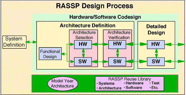
The innovative processes and tools developed under the RASSP program were used to attack the design challenge established by the BM4 SAIP requirements. RASSP's integrated hardware /software codesign process was used to develop a program plan for achieving the BM4 development goals. RASSP's risk retirement spiral process was applied to identify and guide the individual system and subsystem development tasks to systematically retire the highest design risks. At the beginning of the program, a baseline system design was established and the highest risk design elements were identified. Risk retirement tasks were established to solve the individual system/subsystem design challenges. To better understand the development process used on the BM4 design effort, the following is a brief overview of the RASSP design process depicted in Figure 3 - 1.
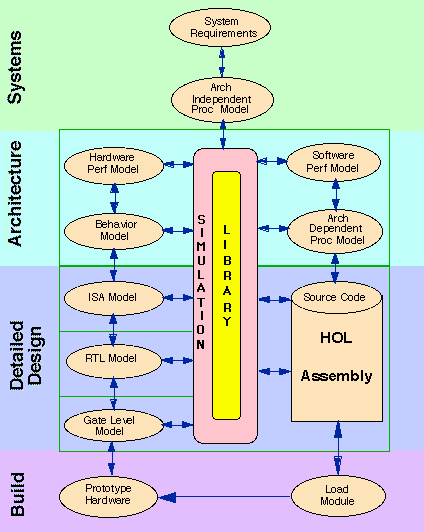
The RASSP development process in based on an integrated hardware/software codesign methodology as compared to standard practice which separates the hardware and software development activities after the initial hardware and software design requirements and specifications are established. In contrast, RASSP's codesign process is partitioned as a function of design abstraction level (i.e. system definition, architecture definition, and detailed design). At each level of abstraction, the hardware and software requirements and design issues are considered jointly. Combined hardware/software design solutions are investigated and developed. Integrated hardware/software virtual prototypes are used to evaluate and verify the evolving hardware/ software designs throughout the process. Figure 3 - 2 shows the various levels and types of hardware/software virtual prototype models that can be used to analyze test and verify candidate designs. Outputs from the design and virtual prototyping efforts are used to make design/cost benefit tradeoffs. Using these hardware/software codesign and virtual prototyping concepts allow developers to identify and resolve hardware/software integration issues throughout the entire development effort, instead waiting until the final hardware/software integration and test phase when problems can have significant cost and schedule impacts.
Within the framework of RASSP's codesign methodology, individual design tasks are established using a risk retirement spiral model. The RASSP spiral model used to accomplish the BM4 SAIP prototype development is shown in Figure 3 - 3.
Each spiral cycle has four phases. In the first phase the baseline design and alternative approaches are identified for each element of the design. In the next phase the candidate designs are evaluated against the system the requirements, alternative approaches and design risks are identified, and risk retirement tasks are defined. In the third phase, design and virtual prototyping tasks are accomplished and results are evaluated to establish the best design approaches for further development. In some instances, design and/or prototyping activities lead to narrowing the hardware/software co-design space, while in other cases, information is discovered which uncovers higher payoff candidates. In the final phase of the spiral cycle, design and virtual prototyping results are reviewed and plans for the next cycle are established. In the course of a development effort "mini-spirals" can be spawned at any time to address critical design issues and retire schedule, cost or technical risks. These "mini-spirals" are focused on developing specific design data and information that is critical for making decisions for the next phase of the development effort.
Each of the individual spiral model tasks or mini-spiral development efforts are focused on providing key design data and information needed to make design/cost benefit tradeoff decisions.
RASSP's methodology makes use of the concept of a expanding design information model where the results from individual design tasks populate the information model. The data accumulated is used to guide subsequent development tasks. As design alternatives are developed and analyzed, the design data is captured to form the basis for critical design decisions. The RASSP expanding information model concept is illustrated in Figure 3 - 4. This model, combined with the risk retirement spiral model, provided the basis for the BM4 development program.
The previous paragraphs provided an overview of key aspects of RASSP signal processing development process. A full description of the RASSP design methodology, processes and work flows can be found in the RASSP Methodology Application Note.
The plan for developing the BM4 SAIP Prototype was based on the BM4 system requirements and RASSP codesign methodology. The baseline architecture was a VME 6U 7 board design with a combination of COTS and custom processors. The BM4 development effort was structured to have a system definition cycle, a architecture design cycle, and a detailed design cycle for implementing the SAIP prototype . During the initial system definition cycle design and risk retirement efforts were focused on establishing the detailed hardware/software requirements and investigating implementation tradeoffs of COTS DSPs versus custom hardware for performing the MSE and HDI processing functions. Table 3 - 1 identifies the key risk retirement activities undertaken during the initial system definition cycle.
System Definition Cycle
The initial task in the System Definition Cycle was the capture and analysis of the SAIP BM4 processor requirements. The top level system requirements were taken or derived from the MIT-LL Benchmark 4 Technical Description (BTD), analyzed and broken down for the BM4 MSE, HDI and control processor subsystems. The individual system and subsystem requirements and specifications were captured in the RASSP RDD-100 system requirement tool. In some instances certain data had to be derived or inferred from the BTD, and/or requested from MIT-LL. Once the system requirements were captured, the individual MSE and HDI subsystem design definition and tradeoff efforts were initiated.
Efforts to analyze the MSE template storage and computation precision requirements resulted in a determination the low resolution templates could be stored as 10 bits and the high resolution templates could be stored with as few a 8 bits. Analysis of the computation precision requirements indicated that performing the computation with 12 bits precision or greater had minimal impacts on classification performance. In addition, to these precision analysis activities, an evaluation of the impact of substituting an Mean Absolute Difference (MAD) computation for the MSE calculation was conducted. This effort showed that classification performance of the MAD and MSE computations were essentially equivalent when compared to target class "ground truth". If anything, the MAD performed slightly better for the BM4 limited test data set. These results were fed back into the MSE custom logic design effort to allow it to be simplified by; reducing the template storage requirements, reducing the precision for the FPGA logic operations and eliminating the need for a multiplier in the MSE computational logic design. A detailed description of the MSE functional analysis efforts is provided in the MSE Classifier Functional Analysis and Implementation section of this Case Study.
Examination of the MSE requirements also uncovered the potential for substantial computational savings over the executable specification implementation. We discovered that incorporating "early termination" logic in the MSE accumulation loop would dramatically reduce the number MSE computations. "Early termination" in effect was the addition of logic in the inter correlation loop to terminate the MSE computation once the best score for a specific chip had been exceeded. While "early termination" greatly reduced the number of pixels processed it complicated the FPGA custom logic design. Based on this discovery a mini-spiral was established to estimate the savings "early termination" could provide. This preliminary analysis indicated greater than 50% savings for the low resolution MSE calculation and more than 40% for high resolution . These results lead to further refinements of the "early termination" approach during the architecture codesign cycle as well as consideration of DSP custom board design candidates for the MSE processor. Additional details of these initial MSE efforts can also be found in the MSE Classifier Functional Analysis and Implementation section of this Case Study.
MSE custom logic design activities during the System Architecture Definition cycle focused on; analyzing and evaluating FPGA custom logic computation and architecture tradeoffs, preliminary parts selection, and initial board layouts. The tradeoff analyses focused on optimizing the computational logic for the MSE calculation and the impacts of template storage and computation precision requirements. These preliminary design tradeoff and sizing efforts, combined with a requirements growth from 10 to 20 target classes, resulted in significant increases over the original estimates of the number of FPGAs and memory chips needed for the custom processor board design. The preliminary design efforts resulted in a projection that three rather than one custom FPGA boards would be required to meet the MSE processing requirements. A detailed description of the MSE custom board development efforts is provided in the MSE Classifier Custom Board Preliminary Design and Implementation Section of this case study.
Results from the MSE functional analysis and preliminary board design efforts were reviewed at the system requirements review and the MSE custom processor design efforts were expanded to include programmable DSP custom board approaches to capitalize on the "early termination" savings. The MSE functional requirements were also relaxed to allow the use of the MAD computation in place of the MSE for the FPGA logic design. These two factors significantly expanded the custom board tradeoff and design activities during the Architecture Hardware/ Software Codesign cycle. Details of these impacts can be found in the MSE Classifier Custom Board Preliminary Design and Implementation Section of this case study.
Detailed review of the HDI processing requirements raised concerns over the efficiency of the original executable specification algorithm implementation. The structure of the executable requirement (three different languages and 39 separate source code files) as well as the complexity of the HDI algorithm made extracting the detailed HDI algorithm functional requirements more difficult than anticipated. As a result, at the end of the initial design cycle, the detailed HDI functional design had not all been captured. The structure of the original HDI code and the computational approach for a number of the algorithm functions showed the potential for significant efficiency gains. Even though the HDI functional analysis had not been completed, initial timing estimates were developed. These initial estimates showed that without optimizing all or parts of the HDI functional code, the number of COTS processor boards required would exceed the baseline system design. On the other hand, restructuring the code and optimizing key functions showed the potential for meeting the four board design goal. A detailed description of the HDI functional analysis efforts is provided in the HDI Functional Analysis Optimizations and Implementation Tradeoffs section of this case study.3.0 The RASSP Development Process Used to Attack the Problem


Critical Design Issues and Risk Retirement Efforts
Finally, the top level system virtual prototype modeling activities resulted in an assessment that the communication requirements between the control processor, HDI processors and MSE processors were low enough that a high speed network interconnect system, like the Mercury Raceway, was unnecessary. However, delays in the HDI functional and communication requirements analysis held up a final decision to eliminate the high speed communication network until data transfer requirements for HDI could be determined.
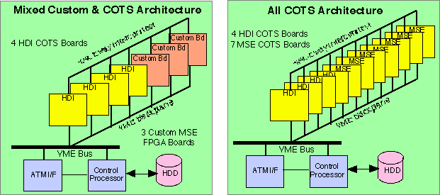
The preliminary results of the System Architecture Definition Cycle were mixed. While there was potential for significant computational savings in both the HDI and MSE implementations, results of the MSE and HDI processor preliminary sizing efforts had lead to an all COTS as well as a mixed COTS/custom logic designs which significantly exceeded the BM4 7 board system design goal. These estimates are reflected in the Mixed and All COTS Architecture candidates illustrated in Figure 3 - 5.
Based on analysis of the System Architecture Definition Cycle design data and results, detailed plans were defined for the Architecture Hardware/Software Co-design Cycle. The MSE custom board design efforts were expanded to include programmable processor custom board design candidates. HDI efforts were concentrated on completing the functional analysis and timing estimates to verify the top level system virtual prototype design results. Efforts to capture the GEDAE™ data flow graph (DFG) primitives for the HDI functions were initiated. The specific design and risk retirement activities defined for this design cycle are tabulated below.
|
Architecture Hardware/Software Codesign Cycle
|
|
The MSE "early termination" refinement effort was established to investigate if greater computational savings could be derived from additional changes to the simple early termination logic used in the earlier design analysis. A number of alternative approaches were evaluated to determine if additional savings could be realized. Details of the individual candidates are described in the MSE Classification Functional Analysis section of this case study. The outcome of these efforts was a final reduction of 65% in the number of pixels processed in low resolution MSE and a savings of 44% in high resolution MSE. The additional savings was realized by reordering the template pixel row vectors from highest to lowest energy content and processing the image chips in the revised order. Overall this resulted in a combined reduction of 2.5x in the computational throughput requirements for low and high resolution MSE processing.
Significantly reducing the MSE computational requirements lead to the potential for performing the MSE function on COTS DSP boards. To investigate this alternative, the "early termination" C code was compiled and run on a COTS Sharc DSP board. The compiled C code required a total of 13.8 clock cycles/pixel during initial testing. Review of the compiled Sharc assembly code indicated it was highly un-optimized. This lead to conducting a two man week effort to develop an optimized MSE Sharc assembly code primitive which required less than 3 clock cycles/pixel. Based on these timing results and the early termination computational efficiency, it was projected that the low and high resolution MSE processing could be performed by 30 or less Sharc DSPs. Analysis of the Sharc memory requirements also confirmed that the templates could all be mapped onto, and loaded in the on chip Sharc memory. Based on available Sharc DSP boards, this meant the MSE function could be performed on two or less COTS boards. This estimate made a COTS board candidate highly competitive with the custom MSE board approaches. It should be noted, in this instance, the investment of 2 man weeks to develop a custom assembly code primitive for the MSE inter loop resulted in a 4.6X reduction in the amount of COTS hardware needed to perform this highly repetitive pixel matching function. Details of the MSE Sharc timing analysis and COTS DSP board estimates are described in the MSE Classifier Functional Analysis and Implementation section of this case study.
During the Architecture Hardware/Software Codesign cycle the HDI implementation efforts were focused on; finalizing the HDI function implementation approach, estimating and verifying runtimes for the HDI algorithm on candidate COTS processor boards and making the selection of the COTS DSP boards for the final system. To accomplish these objectives, a Sun Workstation test bench was developed to test and analyze the performance of alternative algorithm implementations, and measure their relative computational timing.
Algorithm optimization efforts were accomplished by iteratively identifying and reducing the largest computation times of the individual HDI functions. The computational approach for the individual code elements were systematically analyzed and refined to reduce their complexity and computation times. The four most significant implementation and timing improvements were; restructuring the HDI loop structure, substituting faster sub-algorithms (e.g. replacing DFTs and time domain filters with FFTs, applying Horner's rule to matrices, etc.), decomposing a large matrix multiply with a factored version to take advantage of matrix symmetries, and replacing the original Singular Value Decomposition (SVD) calculation with a more efficient Modified Graham-Schmidt (MGS) routine. These along with other implementation improvements resulted in the runtime and operation count reductions shown in figure 3 - 6 and table 3 - 3..


| | ||||||||||||||||||||||||||
| Original Algorithm | ATL Optimized Version | Ratio | ||||||||||||||||||||||||
| Decomp 45.7 | Decomp 6.3 | 7.3:1 | ||||||||||||||||||||||||
| SVD 23.57 | MGS 4.1 | 5.7:1 | ||||||||||||||||||||||||
| Invert 1 | ||||||||||||||||||||||||||
| Backsolve 0.3 | ||||||||||||||||||||||||||
| MLM 7.7 | MLM 11.4 | 0.7:1 | ||||||||||||||||||||||||
| FFT 5.8 | FFT 3.0 | 1.9:1 | ||||||||||||||||||||||||
| Decimate 0.8 | Decimate 0.5 | 1.6:1 | ||||||||||||||||||||||||
| Miscellaneous 7.1 | Miscellaneous 2.5 | 2.8:1 | ||||||||||||||||||||||||
| Total 85.0 | Total 26.2 | 3.3:1 | ||||||||||||||||||||||||
In addition to computational savings, algorithm optimizations also reduced the total memory requirements from 3 Mbytes to 200 Kbytes. This meant the code for HDI would fit in the internal cache memory of a Sharc processor. This eliminated the need for external memory or a high speed communication network to perform the HDI function. As a result, these two requirements were eliminated and available COTS DSP boards were evaluated to determine the best candidate for implementing the SAIP prototype system.
The optimized HDI code was analyzed to determine the relative runtimes and efficiencies for the available COTS DSP board candidates. Candidates included Mercury's i860, Sharc and power PC boards, Ixthos' Sharc boards and Alex Computer Systems' Sharc boards. Initial investigations focused on the efficiency of the DSPs for performing the HDI function. These evaluations resulted in timing estimates for the individual processors using vendor timing data , benchmark timing measurements for critical HDI functions, and iteration counts provided by the HDI testbench. The results of these timing evaluations and the analysis of the number of boards required for the HDI subsystem are summarized in the table below. While the power PC was roughly twice as fast as the Sharc and i860, available COTS boards provided only 4 power PCs versus a candidate Sharc board with 18 processors. Similarly, the highest density i860 board had only 12 processors.
| | ||||
| PE | Estimated HDI Runtime (Secs) | Number of PEs Req'd | Number of PEs / Board | Number of Boards / Cost |
| i860 | 1.6 | 48 | 12 | 4 (med) |
| Sharc | 1.5 | 45 | 18 | 2.5 (low) |
| PowerPC | 0.8 | 24 | 4 | 4 (med) |
The final tradeoffs for the COTS HDI boards resulted in a selection of the Alex Computer Systems 18 processor Sharc board. The Alex configuration was selected based on the DSP board density and relative costs. The summary of the Sharc board candidates and the processor requirements which went into this decision is shown below.
| |
|
|
||
Processors per Board |
| |||
| Communication Network | |
|||
| External Board Memory Rqmts | | | ||
| External Sharc Memory Rqmts |
| |||
| Cost per Board | |
|||
| Cost per Sharc |
||||
Total Hardware Cost |
As a result of the HDI optimization efforts and the selection of the Alex Sharc boards, at the end of the Architecture Hardware/Software Codesign cycle the HDI processor design had dropped from 4 boards to 2.5 boards. Additional details on the algorithm computational efficiency improvement and HDI COTS boards tradeoff efforts are provided in the HDI Functional Analysis Optimization and Implementation Tradeoffs section of the case study.
During the early part of the Architecture Codesign cycle a top level definition of the HDI data flow and the HDI image chip preprocessing functions were defined and established. In an effort to make up for some of the time delays in the HDI functional analysis task, efforts were initiated to develop the HDI data flow graph (DFG). These efforts were focused on capturing the top level DFG, and identifying and developing the primitives needed for the HDI preprocessing functions. After defining the top level DFG, efforts were directed at translating the C code for the HDI preprocessing to GEDAE™ DFGs. These initial efforts emphasized making maximum use of existing GEDAE™ library primitives. The emphasis on maximizing the use GEDAE™ library primitives created several problems.
Some of the preprocessing functions required complicated, HDI specific, indexing, sampling and mathematical functions that did not exist as higher level primitives in GEDAE™s function library. As a result, these unique functions were captured as DFGs using very low level library primitives (e.g. add, subtract, etc.). This approach lead to highly complicated DFGs with multiple levels of hierarchy which were difficult to follow or understand. These complicated DFGs later resulted in extremely large GEDAE execution schedules and lead to program memory problems. To resolve the latter problem, many of these original HDI DFGs were replaced by higher level HDI specific primitives which were not only more understandable but significantly more efficient. Additional details on the GEDAE DFG development efforts is provided in the HDI Data Flow Graph Development and Integration section of the case study.
As a result of the MSE functional analysis and the initial MSE custom board design results, the MSE custom board design efforts were significantly expanded during the Architecture Codesign cycle. In addition to looking at an updated FPGA design using the MAD algorithms, preliminary development efforts were added to evaluate programmable DSP custom board designs. The initial DSP board approach was focused on the TI c80 DSP but was later expanded to include the TI C6201 processor when software development risk and long term product support issues arose with the c80. The custom board preliminary design activities included;
| FPGA | c80 | c80 | c6201 | |
| Design Factor | (40 Mhz) | (40 Mhz) | (60 Mhz) | (200 Mhz) |
| # Processors Per Board | 6 | 4 | 4 | 6 |
| Processor Rate (chips/sec/board) | 17.5 | 7 | 25 | 31 |
| Bus Utilization (%) | N/A | 10.3 | 10.8 | 11.1 |
| Processor Utilization (%) | 89/57* | 94 | 94 | 96 |
| Custom Board Approach | Number of Processors per Board | Board Packaging Density (%) | Cost per Board | |
| Price | SavanSys | |||
| FPGA w/DMA | 6 | 64.6 | 5,709 | 5,145 |
| FPGA wo/DMA | 6 | 61.3 | 5,430 | 4,813 |
| Mezzanine w/DMA | ------ | 49.1 | ----- | ----- |
| c80 (60 Mhz) w/RACEway | 4 | 76.2 | 3,810 | 3,864 |
| c80 (60 Mhz) wo/RACEway | 4 | 69.1 | 3,740 | 3,598 |
| c6201 (200 Mhz) | 6 | 67.3 | 3,970 | 3,736 |
The final results showed the revised MAD FPGA, the c80 (40 Mhz) and the c80 (60 Mhz) custom board designs all required two boards to meet the BM4 30 image chip per second requirement. Only the c6201 design met the requirement (31 chips per second) on a single board. On the negative side, the c6201 was just being introduced in limited quantities and required a significant software development as well as custom board detailed design, fabrication and integration effort. At the system architecture review the custom board design data, along with the MSE COTS approach, were presented. At the review it was decided that the costs and risks associated with the c6201 outweighed the need for the single board solution and the two board COTS solution was selected. Details of the MSE custom board architecture development activities can be found in the Mean Square Error (MSE) Classifier Custom Board Preliminary Design and Implementation Tradeoffs section of this Case Study. Specific details for the FPGA, c80 and C6201 board virtual prototyping efforts can be found in the MSE/MAD Classifier FPGA Custom Board Performance Modeling section and MSE Classifier C80 and C6201 Custom Board Performance Modeling
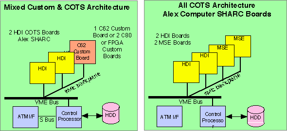
The mixed COTS/Custom Architecture and All COTS Architecture designs resulting from the Architecture Hardware/Software Codesign cycle are depicted below. MSE and HDI functional analysis and optimization efforts had resulted in a 4 board Alex Computer System board design (72 Sharc DSPs). While the c6201 mixed COTS/Custom design potentially had one less board, the cost and schedule risks for the custom design combined with the risk of implementing HDI on only 36 processors resulted in the COTS/Custom design approach being eliminated.
The Architecture Hardware/Software Codesign activities dramatically impacted on the size, cost, and risk associated with the designs at the start of the architecture codesign cycle. Expanded functional analysis and optimization activities had led to significant reductions in the computational requirements. These reductions were enabled by RASSP's codesign process which extended hardware/software requirements and implementation tradeoffs through the architecture design and detailed design cycles. Virtual prototyping activities provided the detailed timing data to make the final BM4 hardware selection and resulted in a hardware solution at one third of the original proposal cost. Based on the results of the Architecture Hardware/Software Codesign cycle, a six board solution (one board less than the design goal of 7 boards) had been identified and efforts could proceed to the detailed design, integration and test cycle.
The primary design/risk issue for the Hardware/Software Detailed Design, Integration and Test cycle was achieving the projected image chip throughput times for the final HDI and MSE real time software. A second issue was developing and integrating the top level HighClass DFG and control program. The final activity required to complete the BM4 prototype development was the procurement, integration and test of the final hardware. To address these design issues and risk areas the following design, integration and test activities were identified for the final Hardware/Software Detailed Design, Integration and Test Cycle.
| Hardware/Software Detailed Design, Integration and Test Cycle Critical Design Issues and Risk Retirement Efforts | |
|
|
|
|
|
|
|
|
|
|
|
|
|
|
|
|
|
|
At the conclusion of the Architecture Hardware/Software Codesign cycle, the final prototype hardware configuration had be defined. Based on the selection of the Alex COTS Sharc boards, orders were placed for the four boards as well as a Sparc 8 control processor, an ATM interface card, the VME chassis, hard disk drive and the workstation peripherals needed to support integration and testing. The hardware used to implement the BM4 prototype is shown in the figure below. The combined cost for the prototype hardware was less than $100K, one third of the original proposal hardware costs.

The initial step in assembling the BM4 prototype was to establish an integration and test environment for the final system. MIT-LL had provide a Sun based Solaris SAIP system emulator and the HighClass executable requirement code. The BM4 system test environment development effort was initiated by integrating the system emulator and HighClass code on two Sun workstations and testing the ATM interface and communication code. Once these interfaces were verified, the BM4 prototype hardware was integrated in the VME chassis. The Sparc control processor and ATM interface were installed and tested with the SAIP emulator and executable requirement software. After successful completion of this step, the individual Alex COTS boards were installed in the chassis and tested. The integration and test of the Alex boards completed the system hardware integration and test environment development efforts and the hardware, shown below, was made available for final DFG development and final integration. Additional details of the BM4 hardware integration and test efforts are described in the HighClass 4 Prototype Hardware Integration and Test section of this case study.
A system level virtual prototype was developed to test and verify the final hardware/software codesign for the BM4 prototype. This model was originally developed using Omniview's Cosmos performance modeling tools. Using Cosmos proved cumbersome and time consuming for modeling the full Alex 4 board, 72 processor system. As a result, only a third of the system was modeled. Subsequently a full 72 processor model was developed using lightweight, token based VHDL models. Using the Cosmos and lightweight VHDL models, DFG mapping and partitioning on the Alex Sharc boards was verified based on image chip timing estimates for the MSE (190 milliseconds) and HDI (1.2 seconds) DFGs. This virtual prototype also allowed us to measure the VME backplane utilization which was relatively low (20%). Finally, the model verified that the Sharc link communication tasks added less than 5 percent overhead. Using the projected MSE and HDI timing estimates the full 72 processor virtual prototype showed the system would meet the 30 image chip per second processing requirements. A thorough discussion of the Cosmos and lightweight VHDL virtual prototyping SAIP HighClass Processor Virtual Prototype Development section.
Efforts on the final MSE DFG development were directed at implementing a efficient, distributed version of the MSE LRC and HRC classification algorithms. Because the template data had to be stored in the on chip memory and the templates for the 20 targets exceeded a single processor SRAM capacity, the LRC algorithm had to be distributed across multiple Sharcs. The distributed LRC DFG was designed to perform the target matches using 4 Sharcs, each containing templates for five target classes. Using the GEDAE and Alex operating system memory management extensions, the target templates were distributed to the LRC processors as large parameter files and stored in specific designated on chip memory locations. Similarly, the since the HRC templates had to be stored in the Alex motherboard DRAM, the HRC DFG was designed to use one of the motherboard root processors compile the HRC template data and send it to the HRC Sharc processors.
The original executable specification contained only ten target classes. Ten additional classes were provided during the detailed design cycle. Analysis of the new template statistics revealed the new classes increased the LRC processing time by 10%. To make up for this increase a change was made to the MSE DFG to increase its' efficiency. The MSE early termination approach results in longer execution times for the early template classes than the later classes. To eliminate this inefficiency, the MSE DFGs were modified to round robin the image chips into the four Sharcs and passing the partial processing results to the next Sharc in the four processor chain. This complicated the DFG but balanced processing times for the individual Sharc processors. This change in the LRC DFG resulted in a 12% efficiency improvement. The final DFG and a trace table showing the execution timing of the four distributed LRC DFG are shown below. This implementation resulted in a processing time of approximately 0.8 seconds per image chip per Sharc and higher than 95% utilization of the LRC Sharc processors for performing the MSE highly repetitive, data intense operation.


Results, of the MSE DFG detailed design effort demonstrated for the first time that highly efficient (as good or better than hand coded) real-time embedded processor code could be generated by an autocoding tool. In addition to providing excellent runtime results, the MSE software made highly efficient use of the on chip memory for image chip and template data caches which were automatically allocated and coded by the GEDAE. The details of the MSE final DFG development efforts and results are described in section 3.1 of the MSE Classifier Functional analysis and Implementation section.
The HDI final DFG development efforts had two critical aspects. The first was restructuring and modifying the earlier HDI DFGs to fit in the Sharc on chip memory. The second challenge was reducing of the HDI run time to less than 1.5 seconds. Once all of the individual HDI DFG processing primitives were captured and tested in GEDAE, the flow graph was compiled and run on a Sharc processor. The Sharc program memory requirements and single chip execution time for this initial HDI DFG were 872 Kbytes (versus the 512 Kbytes available) and 4.2 seconds respectively. Both of these were significantly above the levels needed to meet the SAIP system requirements.
The initial testing pointed out two major factors standing in the way of achieving the memory reduction needed to meet the SAIP requirements. GEDAE provided little insight or control of the embedded processor memory allocation. In addition, the Alex operating system did not allow specific allocation of the Sharc on chip SRAM. Both of these fundamental problems had to be corrected to allow HDI memory optimizations to be accomplished. As a result, efforts were initiated at both Alex and ATL to make the necessary changes in the operating system and autocoding software.
While these efforts were being accomplished, the HDI DFGs were reviewed to identify other changes needed to reduce memory usage and runtime. This review uncovered that restructuring the HDI DFGs to remove the family notation, and replacing as many as possible C code functions with optimized vector library functions would result in both memory savings and run time reductions. The use of families for functions mapped on a single processor results in multiple instantiations of the function code for each family member and drives up memory usage. Replacement of C function code with optimized vector library routines reduces the program memory and provides a path to faster runtime execution. As a result, the HDI DFGs were modified to incorporate these changes.
Testing of the modified DFGs showed memory usage had dropped to 724 Kbytes and runtime decreased to 2.97 seconds. Because of the Sharc memory constraints, the DFG was still using off chip memory and the optimized Sharc library functions were not able to make use of the Sharc's dual operand fetch capability. Projections indicated that using the optimized, multiple fetch functions the HDI runtime would drop to approximately 2 seconds.
The final optimization of the HDI DFG focused on reducing memory use. The GEDAE and the Alex operating system enhancements were used to identify changes to the DFG, GEDAE and embedded processor port software to needed to reduce the on chip memory requirements. Changes were made to GEDAE to allow functions to be executed in place, eliminating the need for two copies of the large HDI data arrays. GEDAE was updated to move the memory allocation function off the embedded processor. Finally, changes were implemented to allow memory to be reused by static sub-schedule functions instead of allocating memory for each subschedule. These three changes resulted in a combined savings of more than 112 Kbytes of on chip memory. In addition, the Alex embedded processor port software was modified to reduce the communications routing table by 60% (from 80 to 34 Kbytes). The remaining memory reductions were accomplished by changing the HDI DFG using GEDAE's enhanced capabilities for displaying and modifying the Sharc SRAM memory map. Overall memory usage was decreased from 724 Kbytes to 456 Kbytes which could be accommodated in the Sharc on chip SRAM.
Once the embedded real-time code fit in the on chip memory, final runtime optimizations could be accomplished. With the incorporation of the optimized dual fetch library functions and several other minor changes, the HDI DFG execution time was reduced to 1.4 seconds.
Optimizing the HDI DFG to fit in the on chip SRAM and achieving execution times of less than 1.5 were significant challenges. The effort was hampered by a need for a number of improvements and extensions to the GEDAE and Alex software. Identifying problems areas and coordinating GEDAE and Alex software enhancement efforts proved to be time consuming and costly. However, in the end, the software tools provided the enhanced memory management and execution control capabilities needed to achieve realtime embedded system requirements. The details of the HDI DFG development activities are described in the HDI DFG Development and Integration section of the case study.
The final software needed for the BM4 prototype was the control program for interfacing the top level GEDAE DFG with the SAIP system. The executable specification software provided by MIT-LL included the original HighClass control code as well as the MSE and HDI functional software. This code used two primary processing procedures, "HighClass" and "Candidate0". HighClass interfaced to the SAIP control system for receiving and sending back "Frame" messages containing image chip processing requests and the output results. HighClass sent individual image chip processing requests to Candidate0 which retrieved the image chips from SAIP's image server, performed the MSE and HDI processing, and returned the classification results and high resolution image chips to HighClass for inclusion in the output "Frame" message. The HighClass code made extensive use of the SAIP "Frame" message data handling routines to extract and input data in the complex C++ "Frame" message data structure. In an effort to minimize the risk of interfacing with the existing SAIP system, extensive use was made of the "HighClass" and "Candidate0" software in the BM4 control program.
The BM4 top level DFG was designed to perform the MSE and HDI image processing functions on a stream of image chips provided by the control program. As a result, the existing HighClass and Candidate0 code had to be modified to retrieve the image chip as part of the control program. HighClass code also had to be modified to; download or change DFG parameters, launch the graph, download the image chip data, and read back the processing results. These code changes were made using a combination of hand coded and autocoded software routines.
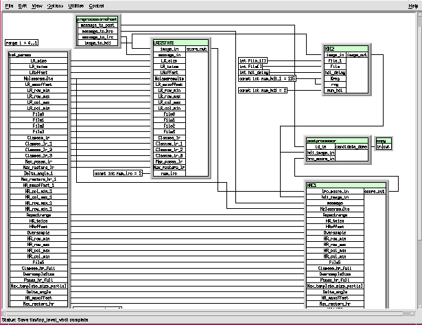
A command language interface is provided with GEDAE for setting DFG parameters and controlling execution when the graph is executed outside the graphical user interface (GUI). As part of the RASSP development effort, an Application Interface Builder (AIB) tool was developed which simplifies coding of these GEDAE command language control functions. In essence, AIB receives information from GEDAE about controllable parameters and provides a mechanism for defining modes and submodes by specifying parameter sets for each mode. In this way the user does not have to explicitly generate the command language code to set all of the 100s of parameters which may be involved with a complicated DFG. In addition, the command program interface provides mechanisms for controlling graph execution and loading and unloading DFG data queues.
Using a combination of hand generated C code and AIB autocode, the executable specification control code was modified to provide the interface between the SAIP system and the HighClass DFG (see illustration below). The control program was structured as three Unix threads. The main thread launched the DFG, processed the incoming and outgoing "Frame" messages, provided DFG mode control, retrieved image chips from the SAIP image server, and serviced the DFG input/output image chip data buffers. Two separate threads were developed for downloading data from the input image chip data buffer into the DFG data queue and uploading MSE and HDI processing results from the DFG output queue into the output results buffer.

The total amount of code required to interface the existing SAIP HighClass code with the BM4 DFG was approximately 1750 lines. Of this total, 750 lines was the existing GEDAE command program interface routines and 500 lines were autocoded by AIB. The remaining 500 lines consisted of 400 lines of code which were modifications of the original MIT-LL HighClass and Candidate0 code and 100 lines were totally new DFG control code.
Once the control program was developed, it was integrated and tested with the system emulator and top level DFG. Initial functional testing of the code was accomplished using the workstation version of the HighClass DFG. Once the functional performance was verified the command program was integrated with the embedded DFG running on the Alex boards. The embedded HighClass DFG was created using a simple timing/data flow version of the top level graph to verify VME data transfer rates. Initial testing uncovered problems with the VME backplane data transfer speed. The problem was isolated to a DMA memory addressing issue on the Alex boards, which was resolved, and the command program ran at over 80 chips per second.
The command program development effort was highly simplified by the use of the GEDAE command program interface and AIB control program autocoding tools. By reworking 400 lines of the existing code and generating 100 lines of new code, the HighClass embedded DFG was interfaced to the existing SAIP control system and provided all of the original SAIP and HighClass control and data handling functions. The details of the approach and activities used to define and implement the BM4 HighClass control program are provided in the SAIP HighClass Control Program Development and Integration section of the case study.
The last task in the BM4 detailed design cycle was the HighClass DFG and control program hardware/ software integration and test. This effort was initiated early using a non-functional version of the top level HighClass DFG. This graph was implemented using an early version of the MSE DFGs and a "virtual HDI" DFG and is shown below. The "virtual HDI" DFG was created by substituting a time delay in place of the functional HDI DFG. When the Alex DSP boards were available, the virtual HDI DFG was partitioned and mapped onto a subset (a total of 28) of the BM4 Sharc processors. Using this top level DFG, a number of GEDAE autocoding, Sharc compiler, Alex operation system and data flow design issues were uncovered and resolved.
These initial DFG integration efforts identified GEDAE extensions needed to provide memory management, parameter file input, cyclic state machine control, and autocode scheduling enhancements. Early identification of the GEDAE extensions provided the lead time for incorporating the changes prior to final DFG optimization. Several bugs were also discovered in the Sharc compiler which lead to changes in the MSE DFGs to avoid the compiler problems. Testing of the HighClass DFG uncovered Alex Sharc board operating system software memory allocation limitations which were identified to Alex. Alex was able to add the necessary features and correct the problems in an undated version of the operating system. Testing of the top level data flow design also identified a problem with the GEDAE Alex board port for the VME direct memory access (DMA) communication software which was corrected. Finally, the top level DFG was invaluable for testing the data flow design and identifying and correcting VME and Sharclink bottlenecks as well as DFG scheduling and queue management design problems.
The ability to test and debug the top level DFG while the final MSE and HDI DFGs were being completed, resulted in the retirement of a number of hardware/ software integration issues prior to final system integration. Using the top level DFG, autocoding tool limitations were identified and corrected, compiler errors were detected and avoided, the COTs board operating system was tested and extended to provide the necessary memory features, and the DFG design itself was modified and updated to achieve the desired performance. Final timing results of the top level DFG running on 28 Sharc processors demonstrated processor utilization of more than 90% (illustrated below) and a throughput rate of approximately 10 image chips per second. A detailed description of the top level DFG development effort can be found in the Final System Hardware/Software Integration and Test section of the Case Study.

The final BM4 hardware software activity focused on integrating the MSE and HDI detailed DFGs in the top level HighClass DFG described above and then integrating this final DFG with the HighClass control program.
Integration of the HighClass DFG for the embedded processor boards was accomplished in two steps. The initial step was the development of an integrated DFG which incorporated the final MSE and HDI DFG but was limited to two families of MSE LRC processors and 16 HDI processors (referred to as the "two family DFG"). This DFG and the mapping of the individual processor functions to the Alex boards are shown below.
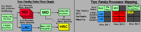
This two family DFG was used to verify the functional performance, develop and test data distribution and queuing functions, isolate and correct problems in the top level data flow design and optimize the graph timing performance. A number of problems were identified and corrected using the two family DFG. Most of the problems were associated with the sizes and locations of data queues between the DFG functions. A second problem was also identified related to the GEDAE Alex board port queue management software which was corrected. The two family DFG optimization efforts resulted in a final timing of HDI function of 1.7 seconds per image chip and an average MSE processing time of 0.8 second per image chip. Once these optimization activities were completed, the final DFG integration and test effort was initiated.
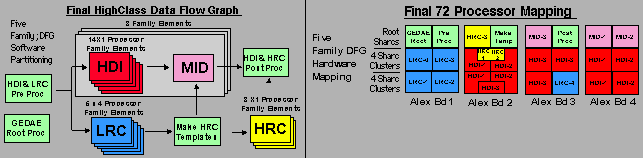
Because of time constraints, it was decided to move from the two family DFG directly to a full 72 processor configuration rather then incrementally building up the number of DFG family elements. Based on the final timing results of the two family DFG, it was apparent the 72 processor system could not achieve the full 30 chips per second processing rate. Since the MSE LRC function was distributed over four processors (each with an average rate of 5 chips per second), the top level DFG was design to have 5 families of the LRC processors which would support an average processing rate of approximately 25 image chips per second. A second change was also made to the top level DFG. The HDI DFG was implemented as three families each having a total of 14 HDI processors and a "mid" processor to gather and assemble the 64 sub images coming out of the HDI processors. The final 72 processor DFG and distribution of the individual functions on the Alex boards are shown below.
The size and complexity of this final DFG presented a number of problems. Initially, we were unable to get the autocode to load and execute on the 72 processor hardware configuration. The DFG was compiling and linking without errors, but the code would not initialize when downloaded to the embedded processors. The problem proved difficult to debug because the DFG would hang during initialization of the preprocessor DSP when trace table data is not available. In an effort to diagnose the problem the DFG was scaled back from 5 families of LRC to 3 families. When this DFG initialized properly, the problem was identified as a communication issue in the preprocessor function. Analysis of this function showed the 5 family DFG preprocessor function had over 180 data ports for transferring data to the HDI and MSE-LRC processors while the 3 family DFG had less 100 data ports. Based on this discovery, the preprocessor function was modified to combine the 3 HDI data ports into a single port reducing the total number of ports to less than 100. This resolved the problem and optimization of the final DFG could began.
The group settings file generated by GEDAE for creating the processors' execution schedules was extremely large (approximately 28000 lines). As a result, the display provided by GEDAE for analyzing and modifying the execution schedule exceeded the X windows display buffer memory limits. To overcome this limitation, a process was developed for converting the group settings file to a Microsoft Excel spreadsheet to review and modify the individual function queues, priorities, and firing granularity settings. This process combined with the hour or so of time required to generate the autocoded schedule slowed progress considerably. Changes to optimize data queue sizes, firing granularity, or individual function priorities were taking 2 to 3 hours. While this seemed quite long relative to smaller DFGs, compared to the normal time required to hand compile, link, load, and execute the code for a 72 processor application, it was a vast improvement. In the end using the GEDAE trace table data to analyze inefficiencies in the 5 family DFG, the final BM4 DFG was developed, optimized and tested in just over 2 weeks which represents a significant improvement over normal hand coded software integration efforts. Additional details on the final hardware/software integration effort can be found in the Final System Hardware/Software Integration and Test section.
Test results for the final HighClass DFG showed the 5 family DFG could process image chips at the rate of 25.4 chips/second. Measurements indicated the processing rate was being limited by the 5 family LRC throughput rate. When this limitation was eliminated by changing the LRC parameters, the DFG run at a rate 26.5 images per second which represented the HDI 42 processor throughput rate. This final HighClass DFG demonstrated 19 percent processor efficiency (intrinsic mathematical operations/peak processing rate) and over 90 percent processor utilization (processor busy). The only efforts remaining after the final DFG integration were the integration of the DFG with the control program and SAIP system emulator.
Once a DFG has been developed and tested, a launch package can be generated to control its execution and modify parameter values. Initial control program integration efforts were accomplished using the two family DFG. This version was used to test and debug the control program, SAIP emulator interface and final acceptance test software. When the five family DFG was completed the control processor was retested with the full graph. Testing the 72 processor DFG uncovered several problems which were corrected prior to acceptance testing. Running under the control program the final BM4 prototype was achieved a 22 image chip per second processing rate. Testing of the control program revealed the thread for reading the DFG output results had irregular execution times indicating the multi-threaded control program was interfering with reading out the results and slowing down the BM4 control program execution. Analysis of the problem it revealed that to correct the problem would require conversion of the control program to a realtime operating system or significant changes to the control processor design, neither of which was an option for the current BM4 development project.
Acceptance testing was accomplished using the five family DFG and BM4 HighClass control program. Acceptance test procedures were executed which measured the all of functional. timing and control performance requirements. Functional performance showed that the BM4 prototype matched 100% (versus a 95% requirement) of the executable specification target classification results. The Sharc single precision classification scores were within .0055 (versus .006 required, under 0.3% error) of the executable specification double precision scores. Visual performance tests performed on the HDI images produced by the BM4 hardware were virtually indistinguishable from the executable specification images. As indicated above the BM4 running with the HighClass control program achieved a sustained throughput rate 22 image chips per second, even though the DFG achieved greater than 25 chips per second. Finally, SAIP mode control function tests demonstrated the BM4 prototype performed all of the SAIP system control functions correctly and interfaced directly with the host system. With the conclusion of the acceptance test the BM4 detailed design, integration and test cycle were completed.
RASSP's risk retirement spiral process and expanding information model was used to establish and guide the BM4 development effort though the system definition, architecture design and detailed design cycles. RASSP's emphasis on system functional analysis and tradeoffs lead to an implementation of the HDI and MSE functions requiring more than 3x less computational throughput than the original algorithm implementation with virtually no impact on functional performance. The hardware/software codesign and virtual prototyping methodology provided the design and verification data for making the cost benefit tradeoffs throughput the process which lead to an all COTS architecture with hardware costs of 1/3 the original estimate. Finally, RASSP's software development and autocoding process and tools demonstrated that a highly complex, distributed signal processing application could be developed and autocoded for a large network of 72 DSPs and achieve as good or better processor/memory utilization and efficiency as current, high cost hand coding processes.
Summary
The RASSP design process was used to develop a highly efficient, low cost processor for performing the SAIP HDI and MSE image processing functions. The final BM4 hardware configuration and characteristics are shown in the figure below.

![]()
![]()
![]()
![]()
Next: 4.0 The Successes, Setbacks and Results of the SAIP Benchmark Development Effort
Up: Case Studies Index
Previous:2.0 The SAIP HighClass Design Problem and Challenges