1.0 Introduction
The SAIP Benchmark 4 (BM4) was established to demonstrate the RASSP methodology for the development of a template-based SAR automatic target recognition (ATR) system. The SAIP system included two subsystems, a High Definition Image (HDI) generator and a MSE Classifier, that were the focus of the BM4 development efforts.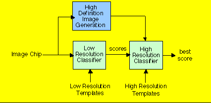
The HDI subsystem generates high resolution images from regions-of-interest or image chips extracted from SAR image frames. The MSE Classifier matches the original chips and their high resolution counterparts to a series of target template sets that include different views (poses) of the targets. The SAIP system was required to process up to 30 image chips/second. The template data base was made up of a set of images for the 20 target classes. Each target class had 72 low and high resolution poses. The low resolution MSE Classifier (MSE-LRC) had to process each chip by matching it against all 72 poses of each target class. The high resolution MSE Classifier (MSE-HRC) then matched the corresponding HDI image chip against 14 poses of the five best MSE-LRC target classes.
The BM4 program was divided into three distinct development cycles: 1) System Architecture Development, 2) Architecture Hardware/Software Codesign and 3) Detailed Design, Integration and Test. The succeeding sections describe the process followed and the results obtained during the MSE Classifier custom board development effort.
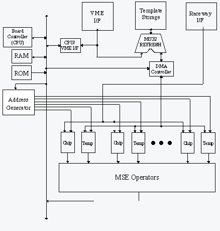
The BM4 design requirements called for the MSE classifier board to process 30 chips per second. Each low resolution chip had to be compared to 20 target classes for 72 poses, at 121 dither locations. Each high resolution chip had to be compared to 5 target classes for 14 poses, at 49 dither locations. The design required on-board storage for the template data, a VME bus interface to the control processor, and a RACEway interface for communicating with the COTS HDI boards.
A key factor in determining the timing performance for alternative board designs was the speed of the custom logic design for computing the MSE scores. This in turn was related to the speed that data could be transferred into the FPGA processors. The basic building block for the MSE custom processor board was the "MSE Operator", shown in figure 3. Several FPGAs components were investigated to determine the best candidate for implementing the MSE Operator. A dual-ported SRAM (DPSRAM) that could provide access speeds comparable to the FPGA also had to be identified.
Since the MSE functional analysis effort {Hot Link} was progressing at the same time the preliminary custom board design computation and template data storage precision requirements had not been established. As a result, the custom board design effort investigated designs for 16-bit, 12-bit, and 8-bit data widths. Template, chip and computation data precision was investigated to determine the top practical speed for the MSE calculation and the number FPGA gates required to perform the MSE computations.
Several logic design alternatives were investigated to determine their impact on board utilization and MSE Operator performance. Two different MSE Operator design configurations were investigated to determine how they affected the number of MSE Operators that would fit on a VME-6U custom board. Processing of the valid and invalid pixels or just the valid pixels was also explored to determine its impact on processor timing and memory storage requirements.
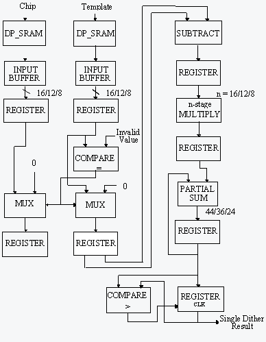
Two MSE Operator design configurations were considered for the custom logic design. The first used a serial partial sum accumulation approach, where each MSE Operator functioned independently and had two DPSRAMs. The second configuration used a parallel partial sum accumulation where 11 MSE Operators were concatenated together. This allowed 11 dither locations to be processed simultaneously. Each set of 11 operators required just two DPSRAMs. Figure 4 shows the basic design of the parallel partial sum accumulation approach.
The precision of the template and chip data had a significant effect on the timing performance and number of gates needed for the MSE Operators. With 16-bit data, the speed of the pipelined operator was limited to 28 MHz because of gate delays associated with the multiplier. With 12-bit and 8-bit data precision, a 40 MHz clock speed could be achieved for the MSE Operators. This was important because DPSRAMs were available for the template and chip caches that would function at 40 MHz. Based on MSE functional analyses {Hot Link}, it was determined that 8-bit data precision generated too many false classifications, but that 10 or 12 bit precision produced acceptable results. As a result, it was determined that a 12-bit logic design would be used. Based on the design for 12-bit data precision, 6 MSE Operators could be implemented on a single FPGA.
The functional analysis had shown that processing only valid data points instead of valid and invalid data points would significantly reduce the number of cycles needed to complete a target match. However, it increased the complexity of the MSE Operator design significantly. After analyzing the logic needed to process only the valid pixels, it was determined that the FPGA gate savings achieved by using 12-bit precision was nullified by the control logic required to bypass invalid data points.
As a result, it was decided that the MSE Operator baseline design would use 12-bit precision and process both valid and invalid data points. Based on this configuration 6 MSE Operators fit on a single FPGA. If serial partial sum accumulation was implemented, then 1 FPGA or 6 operators fit on a single board. This constraint arose from the fact that 12 DPSRAMs were needed to support the six operators. However, if parallel partial sum accumulation was implemented, 3 MSE Compute Elements or 33 operators fit on a single board. Based on the denser packaging, the parallel partial sum design was chosen as the best custom logic computational approach. The MSE Compute Element was implemented with two FPGAs and two DPSRAMs.
A summary of the preliminary timing and layout analysis is provided below. The table shows the number of FPGA custom boards required to execute the MSE LRC and HRC computations at 30 image chips per second. As shown, all of the custom board design candidates exceeded the single board design goals established for the BM4 SAIP processor. In addition, since twelve bit precision was needed to meet the MSE classification accuracy requirement be best solution was the 12 bit, Parallel Partial Sum Accumulation approach which required 2.3 (actually 3) VME-6U boards.
At the conclusion of System Definition Design cycle, the preliminary custom board design tradeoffs had led to an expanded, unacceptable 3 board solution for performing the MSE target classification function. This was partially due to the increase from the original ten target classes that doubled the template storage and processing requirements, and partly attributable to underestimating the number of FPGA gates needed to perform the MSE calculations. However, concurrent with the custom board preliminary design effort, the MSE functional analysis activities (Hot Link) had analyzed replacing the MSE computation with a Mean Absolute Difference (MAD) computation. This had little, if any effect on the target classification performance. Functional analysis efforts had also discovered that an early termination strategy to control the MSE computation loop could lead to 50% or greater reduction in the number of pixels processed. These two design factors along with the preliminary custom board design data were considered in establishing the critical design issues and risk reduction tasks for the Architecture Hardware/Software Codesign phase of the MSE custom board development effort
The potential benefits of the MAD calculation and early termination provided a good argument for revisiting the FPGA-based classifier design. They also lead to expanding the custom board candidates to include programmable custom board approaches. After searching for the appropriate FPGAs and programmable CPUs, the list of design candidates was narrowed down to an ORCA FPGA, a comparable FPGA from Actel and the TMS320C80 Multimedia Video Processor (MVP) from Texas Instruments (TI). During the initial design phase of the c80-based classifier design, concerns arose about programming the c80, which requires two compilers, as well as TI's future support of the c80 product line. These concerns resulted in the TI TMS320C6201 fixed-point DSP being added to the list of candidate processors.
During this phase, the FPGA logic designs were updated to reflect the MAD computation and parts lists for all of the processor alternatives were developed. Using these parts lists a board layout of each design was captured, a board level cost estimate was generated and a virtual prototype for each design was developed.
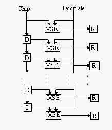
Early termination was also considered for the FPGA logic design. For the parallel partial sum accumulation approach, all 11 MAD Operators of the compute element operate in tandem and are controlled by the same clock. Execution of a single operator cannot be halted early and restarted with new pose data unless all eleven operations are halted and restarted at the same time. This eliminated most of the potential advantage for the early termination computational savings for the FPGA parallel partial sum accumulation design.
The serial partial sum accumulation configuration was also revisited to investigate the addition of early termination. In this situation, a single compute element operates independent of the others and its execution can be halted without affecting the output of the other compute elements. However again, due to the amount of board space consumed by the DPSRAMs for this approach, only 7 compute elements could be fit on a single VME board. As a result, the parallel partial sum accumulation approach using the MAD computation, 12 bit precision, valid and invalid pixels, and without early termination were established as the most compact FPGA design approach.
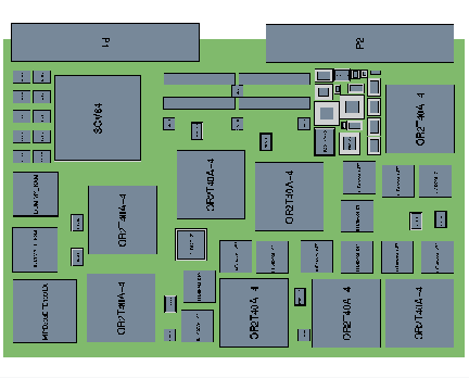
Based on this design a preliminary board layout was captured with the SavanSys hardware design tools (see figure 5). The Savansys tools are designed for early capture and layout of an electronic module or MCM design. They also provide estimates of the module production costs. Finally, the SavanSys tools interface directly to the Mentor hardware design tools for the final detailed hardware design. The illustration below shows the SavanSys preliminary layout of the FPGA VME-6U design. The template storage memory was located on a separate mezzanine card. The remainder of the design occupies about 65% of the usable board space.
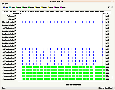
The FPGA board design was modeled using OmniviewŐs Cosmos. The figures 6 and 7 show the Cosmos hardware model and timing results for the Cosmos FPGA custom board virtual prototype (Hot Link). Additional details on the MSE FPGA virtual prototype can be found in the virtual prototype section of this case study. Using the Cosmos virtual prototype the parallel partial sum accumulation throughput performance was verified to be significantly more efficient than the serial partial sum accumulation with early termination. The model also established that a single board using the parallel partial sum approach could process 30 chips in 1.71 seconds. Based on these modeling results two FGPA
custom boards were required to meet the SAIP 30 chip per second requirement. Timing tests of the virtual prototype for the serial design, with early termination, showed that three boards would be required to process 30 chips per 1 second. As a result, the best custom logic solution was the parallel partial sum accumulation approach that could meet the SAIP specifications using two boards.
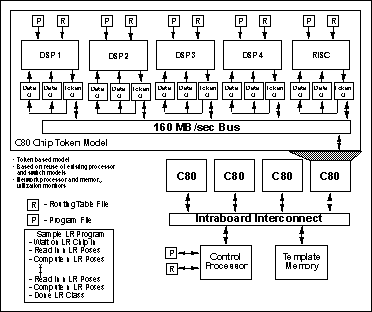
The c80 has a multiprocessor architecture that includes four 32-bit, fixed-point DSPs and a 32-bit floating-point RISC control processor. Each DSP has 2K Bytes of instruction RAM, 6K Bytes of data RAM and 2K Bytes of parameter RAM. The c80 includes a video controller and a transfer controller that provides a 64-bit programmable interface to external memory and programmable DMA access to all internal memory. The internal bus is a 64-bit crossbar that interconnects all of the internal chip components.
Given the computational resources available on each of the c80 DSPs, there were several approaches for implementing the MSE or MAD calculations. These alternatives are highlighted in table below. The efficiency of each approach was evaluated using an estimate of the inner loop cycle times. The inner loop was the part of the code that executes the MSE or MAD calculation on a steam of template and image chip pixels. As can be seen, the inner loop throughput varied from 0.5 cycles/data point up to 1.5 cycles/data point. The throughput was affected by the precision of the data points, which was in turn directly related to the way the ALU was used. The Data Unit ALU can be configured as a 32-bit fixed-point ALU, split into two 16-bit ALUs or split into four 8-bit ALUs. If the ALU is split, all sub-ALUs must execute the same instruction at the same time and the data must be unsigned, positive values.
The second method, based on the MAD calculation using 8-bit input data, was dismissed because system analysis had shown an unacceptable degradation in the classification results.
The first method calculated MSE values using 16-bit input data and the third method calculated MAD values using 16-bit precision. A difference between these two implementations was that the MAD calculation requires the use of positive, unsigned values. The SAIP template and image chip data included both positive and negative values. As a result, offsetting all of the data before or during the generation of the correlation values added overhead cycles and increased the total computational complexity.
A second difference between these two approaches was the reduction in number of pixels processed using the early termination threshold control. For MSE the difference between the chip and template data points is squared. This results in the best (lowest) scores being exceeded more quickly and results in greater early termination computational savings. For these reasons, the MSE calculation was chosen over the MAD calculation.
While the inter loop timing performance estimates of the c80 was 1.5 cycles/sec, they did not include loop control overhead, internal data RAM access contention, and software pipelining. These overhead functions were directly effected by the length of the pixel vectors being processed. As the vector size increases, the overhead drops and the inner loop throughput estimate approaches the 1.5 cycles per second limit. For low resolution processing, where the average vector length was 11 pixels, the throughput rate with overhead was estimated to be 3.2 cycles/ data point. For high resolution processing, where the average vector length was 27 pixels, the throughput was estimated to be 2.12 cycles/second.
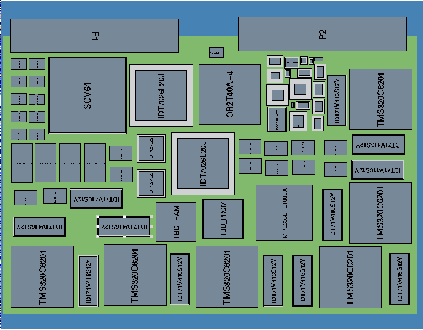
The c80 board layout was also captured using SavanSys tools described earlier. The template storage memory components were replaced with higher density, higher speed chips than those used on the FPGA custom board. This eliminated the need for a separate mezzanine card. Using a preliminary parts list a layout was developed which accommodated 4 c80 MSE processing elements on a single board. This layout, shown in figure 8, used 69% of the available VME-6U board space.
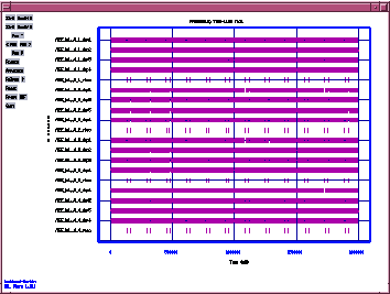
To model the c80 board design, a custom lightweight VHDL model was developed. The c80 VHDL virtual prototype used a model of the c80 based on its internal chip components. Figures 9 and 10 show the basic architecture of the c80 custom board model and the resulting timing performance. Additional details on the MSE c80 virtual prototype can be found in the virtual prototype section of this case study
{HOT LINK}. Results of the c80 virtual prototype the timing simulations established that a single board could process 25 image chips per second. Based on these modeling results two c80 MSE custom boards were required to meet the SAIP requirement.
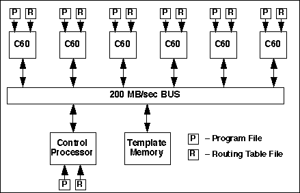
The c6201 is a 200 MHz, 32-bit fixed-point digital signal processor architecture based on a Very Long Instruction Word (VLIW) CPU core that includes eight function units that can operate simultaneously. The internal memory of the c6201 can be divided into Data RAM and Program/Cache RAM. The density of the Data RAM is 64 Kbytes and can be viewed as eight columns that are one byte wide, where memory addresses can be interleaved across consecutive columns. The Program/Cache RAM is configured as a 2k x 256-bit memory so each VLIW fetch instruction can be accessed in a single cycle.
In a fashion similar to the c80 design, the number of cycles for performing the MSE inter loop was determined and the overhead for loop control and data transfer was estimated. The compute time for low resolution processing was 3.47 cycles/data point. For high resolution processing it dropped to 1.85 cycles/data point. The rate of transfer of data into internal data RAM was 200 Mbytes/second. Contrary to the c80-based design which was memory limited, each c6201 could process a complete chip; matching it against all low resolution and high resolution poses.
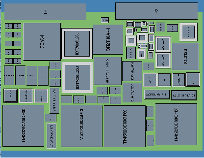
Using the SavanSys tools a preliminary layout was developed for the c6201. Because the c6201 had a smaller footprint than the c80, six of the 200 MHz c6201s with their external memory fit in the same space as four c80s (see figure 11). Again, a mezzanine card was not required for the template storage memory. This preliminary board layout resulted in 67% utilization of the available VME-6U board space.
Using a simplified version (see figure 12) of the c80 token based VHDL virtual prototype, the performance of the c6201 custom board was modeled and evaluated. Results (see figure 13) of these simulations established a single VME-6U board with six c6201s could process 31 image chips per second.
The board costs were estimated using both the Price M Model and SavanSys tools. Even though the costs differ slightly between the two tools, the trends are the same. The FPGA board design was the most expensive approach, and these estimates do not reflect the added cost of the mezzanine card. The least expensive approach was the c80-based design that does not require an interface to the RACEway.
At the beginning of the MSE custom design effort, a board utilization criteria was established which stated that the set of components for any of the design approaches will not cover more than 75% of the available board space. This criteria was met in all but one instance where a RACEway interface was included. Board layouts were captured with and without the RACEway interface because the final system bandwidth requirements had not been resolved at the time the classifier board design tradeoffs were being investigated. It was later determined that the RACEway interface was not required.
From a performance, size and cost perspective, the best choice for the MSE custom board design was a c6201 implementation because it was the only candidate which met the system 30 chips/second processing requirement on a single VME board. The c6201 board estimated production cost also fell at the lower end of the production cost scale. One drawback for using the c6201 was that production components were not available from TI and the software development environment was new and immature. These factors represented both cost and schedule risks for completing the detailed design, integration and test of the MSE custom board.
Concurrent with the custom board preliminary design efforts, the MSE functional implementation tradeoffs and a preliminary software development effort to evaluate the performance of a COTS Sharc DSP implementation had lead to a determination that a two board COTS solution could be achieved. As a result, the COTS candidate was added to final MSE processor tradeoff analysis and selection. Because of the uncertainty of c6201 parts availability, the software maturity, and the non-recurring costs to implement a custom board, it was determined that a COTS, two board solution was the most cost effective, lowest risk approach for meeting the MSE processing requirements. As a result, at the conclusion of the Architecture Hardware/Software Codesign cycle, the MSE custom board development effort was terminated and the MSE processor detailed design efforts were refocused on developing the software for the COTS Sharc boards.
In summary, during the Architecture Hardware/Software Codesign cycle RASSPŐs virtual prototyping and preliminary hardware design tools were used to develop and analyze the designs for multiple FPGA and DSP design alternatives. Virtual prototyping efforts, using Cosmos as well as in-house VHDL modeling tools allowed us to thoroughly evaluate the relative performance of these custom logic DSP board designs. RASSPŐs tools and techniques allowed us to develop detailed models of the individual design candidates and generate reliable performance estimates for each of the designs in a matter of weeks. Preliminary hardware designs and parts lists were developed and used to establish preliminary board layouts and production cost estimates for each of designs. Combined, the RASSP performance modeling and hardware design processes and tools provided the detailed design information needed to make the final MSE processor hardware design selection. The detailed performance, size and cost data provided by RASSPŐs hardware/software codesign processes and tools resulted in identify the most cost effective design approach and avoiding the recurring cost and risks of a custom board hardware development effort.
2.0 System Architecture Development
Custom Board Preliminary Design Tradeoff Analyses
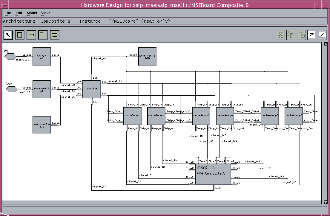
At the start of the custom MSE board development a top level board architecture was defined that identified all the major functions and a notional description of its operation. This architecture, illustrated below, was based on the original MSE algorithm requirements found in the BM4 Technical Description (BTD). A preliminary design analysis and tradeoff study was then conducted for the MSE board. This analysis focused on estimating the speed and hardware resources needed to meet the MSE-LRC and MSE-HRC functional requirements. The preliminary design efforts concentrated on a custom FPGA board design to perform the MSE processing. The baseline FPGA MSE custom board design is shown in figure 2. Design efforts were focused on defining the best gate level logic implementation for performing the MSE classification function, estimating the number of gates required, identifying the critical components for the other board functions, and developing a preliminary board layout.
(Number of Boards Required to Meet 30 Chip Throughput Requirement) 12 Bit Data Precision 8 Bit Data Precision Serial (Valid data only) 6.3 5.4 Serial (Valid and Invalid) 4.0 3.5 Parallel (Valid and Invalid data) 2.3 1.75 3.0 Preliminary Design of Classifier Custom Board
At the time of the Architecture Review, the use of the Mean Absolute Difference (MAD) calculation in place of the MSE calculation along with the use of early termination were being investigated as part of the MSE functional analysis effort (Hot Link). The initial investigations showed that use of MAD caused no degradation in the classification results and the use of early termination dramatically reduced the number of calculations needed to meet the MSE target classification specifications.
3.1. FPGA-Based Preliminary Design
After further analysis, it was determined that the Lucent Technologies OR2T40A FPGA was the best choice for the custom FPGA design approach. The implementation of MAD custom logic approach dramatically affected the number of gates needed for the computation as well as FPGA board throughput. The MAD calculation does not require the multiplier that represented 85% of the gate level logic required for a single MSE operator. Using the MAD computation and 12-bit data precision, 11 operators could be implemented on a single FPGA and a MAD Compute Element could be implemented with 1 FPGA and 2 DPSRAMS. The equivalent MSE Compute Element required 2 FPGAs and 2 DPSRAMs. The MAD design for the FPGA used only 50% of the available logic gates. This low level of gate utilization provided a high degree of confidence that estimated propagation and routing delays could be achieved using automated design tools. Using this logic design, 6 compute elements, or 66 MAD operators fit on a single VME board.
C80 BASED PRELIMINARY DESIGN
Because the functional analysis had shown that early termination and processing only valid data points dramatically decreased the number of calculations required to process 30 chips per second, custom board designs with programmable DSPs needed to be investigated. After an initial search of RISCs, DSPs and even MACs, the TMS320C80 Multimedia Video Processor (MVP) was selected as the best candidate for a programmable custom board design.
Computation Approach On Chip Resources Data Size Inter Loop Throughput MSE
MAD
MAD
3.3 c6201 BASED PRELIMINARY DESIGN
The TMS320C6201 was a late addition to the list of processors considered for the MSE custom board design. It was added as an alternative because of the software and long term support issues associated with the c80 described above. On the other hand, TI had announced they expected to double the speed of the emerging c6201 product line in 1999, and a floating point version of the architecture was also under development.
4.0 Classifier Custom Board Preliminary Design Summary
The preliminary MSE custom board design effort resulted in board designs, performance simulations and production cost estimates for each of the custom board design candidates. The final selection came down to the board level performance analysis and the number of boards needed to meet the 30 chips/ second requirement. The following table provides a comparison of the board layouts, and production cost estimates and performance modeling results.
Custom Board Approach Number of Processors per Board Board Packaging Density
Cost per Board Price SavanSys FPGA w/DMA 6 64.6% 5,709 5,145 FPGA wo/DMA 6 61.3% 5,430 4,813
Mezzanine w/DMA ------ 49.1% ----- ----- c80 (60 Mhz) w/RACEway 4 76.2% 3,810 3,864
c80 (60 Mhz) wo/RACEway 4 69.1% 3,740 3,598
c6201 (200 Mhz) 6 67.3% 3,970 3,736
FPGA c80 c80 c6201 Design Factor (40 Mhz) (40 Mhz) (60 Mhz) (200 Mhz) # Processors Per Board 6 4 4 6 Processor Rate 17.5 17 25 31 (chips/sec/board) Bus Utilization (%) N/A 10.3 10.8 11.1 Processor Utilization (%) 89/57* 94 94 96 Note: * low resolution/high resolution