Next: 6 Integration and Test Up: Case Studies Index Previous:4 Architecture Design
![]()
![]()
![]()
![]()
Next: 6 Integration and Test
Up: Case Studies Index
Previous:4 Architecture Design
Because most of the software developments were verified during the architecture process,
software developments in the detailed-design-process step were limited to creating those
elements that were target-specific: configuration files, bootstrap and download code, target-
specific test code, etc.
The top level of a detailed, behavioral, virtual prototype was a structural VHDL model
defining interconnection between individual elements that made up the system, board, or
module being modeled ( Figure 5- 2). The element models at the lowest level of the
hierarchy were behavioral models that described function and timing, with typical lowest
level elements being Application-Specific Integrated Circuits (ASICs), Programmable
Logic Devices (PLD), memories, and Commercial, Off-The-Shelf (COTS) components.
The COTS component could either be a chip or several chips packaged together, such as a
Multi-chip Module (MCM).
The structural model at the top level of the detailed, behavioral, virtual prototype allowed
the interchange of different models for the same element. For example, in the early stages
of the design, functions may not have been partitioned between individual components
[ASICs, Field-Programmable Gate Arrays (FPGA), PALS, etc.], and may be modeled by
one composite component. Once designers partitioned the functions into individual
components, they extended the structural model down an additional level of hierarchy.
Post-synthesis models of custom components were used for component design verification
in the virtual prototype. Data resolution on the signals between elements was bit-true. The
simulation yielded the signal logic values as they would appear in the hardware when
executing the same software function. A VHDL testbench applied stimulus to the VHDL
model during simulation, and compared simulation outputs to the expected outputs.
The detailed, behavioral ,virtual prototype can perform timing analysis at two levels: Cycle
true timing checked the time sequencing of events or signals on a cycle-by-cycle basis,
such as bus-interface protocol. The second level of timing analysis checked timing within a
clock cycle. This required that the component models included timing information, such as
output-signal propagation delays, set-up times, and hold times. The simulations can
investigate the impact of clock frequency and skew variations. A special case of clock-
skew-variation investigation was simulation of systems with two or more independent
clocks.
A virtual prototype was developed for the Data I/O board but not for the other boards in the
SAR processor. The Data I/O board was a new board design, while the processor boards
and host interface board were COTS boards, requiring no new hardware design. The
purpose of the virtual prototype of the Data I/O board was to verify the correctness of the
hardware design and hardware/software interaction. The virtual prototype also served as a
platform for defining two new FPGAs developed for the Data I/O board. During the test
and integration of the SAR's hardware/software, the virtual prototype was used to
investigate anomalies and to verify changes before they were made to the hardware. The
virtual prototype also served as design documentation for the Data I/O board.
The component models were at the lowest level in the model hierarchy. Only the
functionality and I/O behavior were modeled for COTS components. Modeling internal
details of COTS components added no value to the virtual prototype and was likely to
increase the time required for a simulation run. The important thing for COTS component
models was that function and timing be accurately modeled at the component I/O interface.
The VHDL models for the two new FPGAs were taken down to the RTL level and
included only constructs that could be handled by FPGA synthesis tools. Developing the
FPGA models directly in synthesizable VHDL eliminated the intermediate step of first
developing a higher level functional model of the FPGA.
The existing components that proved most difficult to model were the two RACEway
FPGAs purchased from Mercury Computer Systems, Inc. Lockheed Martin Advanced
Technology Laboratories (LM ATL) used proprietary information from Mercury to develop
models for these two ASICs at the RTL level. This information was in the form of
schematics and partial VHDL. Modeling to the RTL level was not required because LM
ATL was not changing the internal design of the FPGAs. However, RTL-level models
were easier than higher level functional models to generate using the information that was
available. A full understanding of the FPGA operation was not required to generate RTL-
level VHDL from the schematics, and all existing VHDL was at the RTL level. There was
no noticeable impact on simulation time resulting from using RTL level models.
The only active components on the Data I/O board that were not included in the structural
model were the Electrically Programmable Read Only Memories (EPROMs) that configured
the FPGAs when power was first applied to the board. The FPGA configuration process
was not modeled because the FPGA models already defined the functionality of the
FPGAs.
One section of the testbench models the VMEbus activity, including writes and reads of
memory-mapped registers on the Data I/O board. The testbench read the FIR filter
coefficients from a file and loaded them into the FIR filter. Changing FIR filter coefficients
between simulation runs did not require any change to the testbench, only a different
coefficient file. Therefore, the software operations of loading FIR filter coefficients,
loading other control registers, and reading status registers over the VMEbus were verified
on the virtual-prototype model of the hardware prior to hardware build.
The simplest form of the testbench operated the Hot Rod fiber-optic interface in loop-back
mode, a valid test mode for the Data I/O board (Figure 5-4). The testbench connected
transmit data back to receive data on the Hot Rod interface. One version of the testbench
supplied input data and captured output data in data files when exercising the Hot Rod
interface. Another testbench operated with the executable-specification testbench as the data
source and sink. These testbenches were used to verify the operation of the Data I/O board
in different simulations.
Both input and output of data were modeled on the RACEway interface port. Data being
applied to the Data I/O board RACEway port was read from one file by the testbench, and
the board's data output to RACEway was stored in another file by the testbench. The
captured data could then be compared with the expected data. The testbench modeled
RACEway protocol and the sequence of operations performed by the software during data
I/O operations. This verified that the RACEway port's hardware would respond correctly
to software-initiated commands and RACEway protocol.
Approximately 782 hours were spent developing and simulating the Data I/O board's
detailed, behavioral, virtual prototype. Much of this time was devoted to the detailed
specification of the two new FPGA designs.
For the SAR processor, it was not necessary to redesign the Data I/O board or its FIR filter
daughter card. The problems encountered during integration and test were due to
manufacturing defects, incorrect or misleading vendor documentation, and synthesis tool
problems. Two wires were added to the Data I/O module as a result of defects found during
test and integration. The first wire corrected a problem resulting from a misinterpretation of
vendor-supplied documentation for the RACEway interface ASICs. The second wire
changed the operation mode of the Hot Rod fiber-optic interface. The Hot Rod was
unreliable in the original operation mode. Both FPGAs were resynthesized during test and
integration along with associated update of the FPGA design documentation.
The Data I/O board design was reviewed for possible testability improvements. The
modifications, which were incorporated into the design, included test modes for counters,
short cycling of counters in test modes, capability to operate with a single external-clock
source, deterministic state at reset, and synchronous operation (whenever possible). A
Joint Test Action Group (JTAG) test port was incorporated into the Data I/O design, and
scan buffers were inserted at strategic points in the data paths. These features enabled test
vectors to be developed for testing either from the JTAG port or by a board tester. All of
these features were modeled and verified in the detailed, behavioral, virtual prototype with
the exception of JTAG. The JTAG was not modeled because it was not used during the
actual hardware test, and it would have required significant additions to the component
models.
The Data I/O module was designed so that manufacturing test vectors could be extracted
from the Data I/O's behavioral, virtual-prototype simulations. The input vectors were
generated by the testbench, and the expected response captured at the interface between the
Data I/O module and the testbench.
Mentor's Design Architect tool was used to capture the schematics detailing the interconnect
between module components. The interconnect was compared for consistency against the
interconnect of the structural VHDL in the top-level ,detailed, behavioral model.
The timing of the Data I/O module was analyzed by adding timing generics to the
component models in the detailed behavioral model. The timing for COTS components was
taken from component data sheets and the timing for the FPGAs was taken from static-
timing analysis of the synthesized FPGAs. The Data I/O module was simulated using
worst-case timing for all components.
A drawing package was created for both board designs that made up the Data I/O module.
This drawing package contained all the information needed to fabricate and assemble the
boards. The Data I/O module design and theory of operation are described in Data I/O
Board Hardware Description and Operation. This document describes all connectors and
I/O signals and memory-mapped registers, and it describes in detail the operation of Data
I/O. It proved invaluable during test and integration.
The FPGA logic was synthesized using Synopsys' FPGA Analyzer tool. The FPGA
VHDL was imported into the Synopsys environment from the Mentor QuickVHDL
environment. which had been used up to this point. This demonstrated an advantage of
using a common language (VHDL) throughout the design process. The Synopsys output
was used as the input to the NeoCAD tool that mapped the synthesized logic to the physical
structure of the ATT2C15 ORCA FPGA. Any changes made in the design for synthesis
purposes were reflected back to the VHDL model in the detailed, behavioral, virtual
prototype. Therefore, all changes were verified in the detailed, behavioral, virtual
prototype.
The Static Timing Analyzer tool in the NeoCAD tool set was used to extract timing
information from the two FPGA designs following placement and route. The extracted
timing was back-annotated by hand into the virtual prototyped FPGA models, and the suite
of simulations were performed again to verify timing at the Data I/O board level. Although
this process verified timing, it did not check functionality of the final hardware
implementation. A consequence was the failure to detect several logic faults introduced by
the tools, and these faults were not found until test and integration
The preferred back-annotation approach would be to extract the structural VHDL model along with a Standard Delay Format (SDF) file from the FPGA layout. The structural model SDF file, and the library of cell primitives for the FPGA technology would then combine to generate the back-annotation model of the FPGA. The virtual-prototype simulations would then be performed with the back-annotation model replacing the originally developed FPGA models. This approach was not taken because the NeoCAD tool did not have VHDL-netlist capability at that time.
design implementation. This verification was possible because the models at both
virtual-prototype levels were developed in a common language (VHDL), and the two
virtual prototypes were developed with a common structural hierarchy.
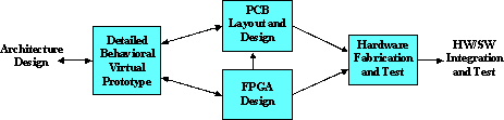
5.0 Detailed Design
5.1 Detailed Design Process Description
During the hardware portion of the detailed design process, behavioral specifications were
transformed into detailed designs [Register Transfer Level (RTL) and/or logic-level] by
combining hardware partitioning, parts selection, and synthesis (Figure 5-1). Detailed
design functionally and performance/timing were verified using detailed behavioral
simulation. The design results were detailed hardware layouts and artwork, netlists, and
test vectors that could be seamlessly transitioned to manufacturing and test via format
conversion of the data.
5.1.1 RASSP Innovations in the Detailed
Design Process
The Rapid Prototyping of Application-Specific Signal Processors (RASSP) process
extended the common-language [VHSIC Hardware Description Language (VHDL)]
hierarchical modeling and simulation to the detailed design process. The detailed behavioral
model, also called the detailed behavioral virtual prototype, was the lowest level in the
simulation-model hierarchy. A primary difference between the detailed behavioral model
and the abstract behavioral model was the level of timing and signal details. The detailed,
behavioral, virtual prototype had a one-to-one correspondence between actual hardware
signals and signals defined in the VHDL models. Timing resolution was taken to timing
within a clock cycle. This enabled the performance and behavior of the hardware to be
simulated at the component and signal levels. Simulations of the detailed behavioral
virtual prototype tended to focus on a specific aspect of the system being designed, rather
than on the entire system, as was the case for the performance and abstract, behavioral,
virtual prototypes.
5.2 Module Design
The SAR processor design required the development of two new Printed Circuit Board
(PCB) designs: Data I/O motherboard and the Finite Impulse Response (FIR) filter
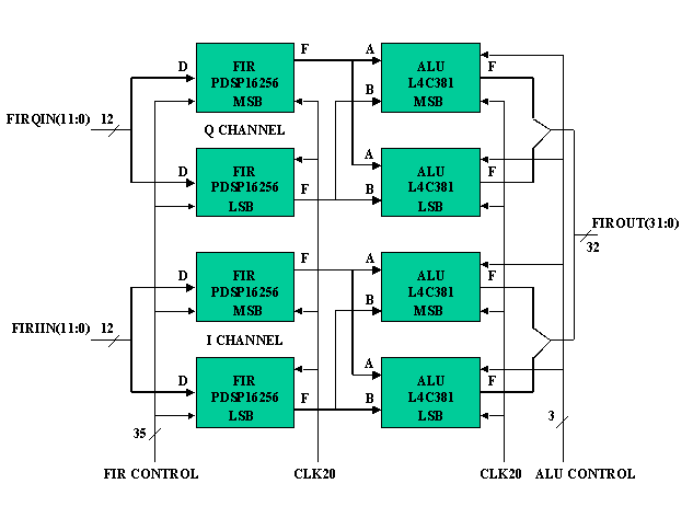
daughter card. The Data I/O board (Figure 5-2) is a 6U VME board with two daughter
cards, Hot Rod Fiber-optic board, and FIR filter board (Figure 5-3). 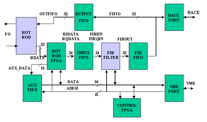
5.2.1 Detailed Behavioral/Register-Transfer-
Level Modeling
Detailed, behavioral, virtual prototyping was used when new hardware was being
developed to facilitate the design process and to reduce the risk of design errors. The
detailed behavioral model differed from the abstract behavioral model in the level of
abstraction. Entities were resolved to the component level in the detailed behavioral model
rather than to the functional unit level of the abstract behavioral model. Signal resolution in
a detailed behavioral model was at the bit-true level, and timing was at either the clock edge
or within the clock cycle. The detailed behavioral model was simulated through its modes
of operation before the hardware was built, thereby minimizing the probability of design
error or incompatibility among components. The term "virtual prototype" is used in this
section to refer to the detailed behavioral model along with its testbenches.
5.2.1.1 Detailed Behavioral Virtual Prototype
Models
The top-level virtual prototype-model was structural VHDL, with each physical component
represented by an instantiation of a component model. Data Input/Output (I/O) components
are First In First Out (FIFOs); FIR chips; ALU chips; FPGAs, etc. This hierarchy in the
virtual prototype made it easy to substitute one component model for another. For example,
most of the component models were generic when the design began. As component
selection proceeded, the generic component VHDL models were replaced with models
having the function and timing of the actual component being used.
5.2.1.2 Detailed Behavioral Virtual Prototype
Simulation
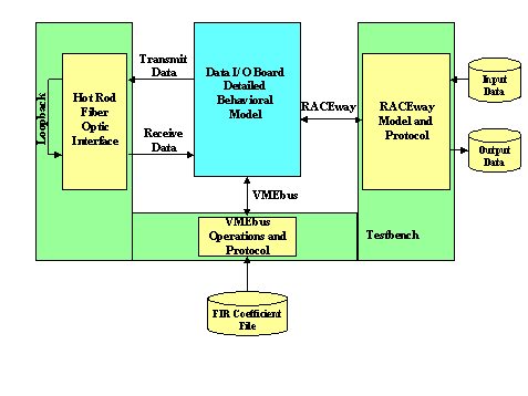
The Data I/O board testbench (Figure 5-4) was designed to exercise the virtual prototype
through its various modes of operation. The testbench generated input signals that were
applied to the Data I/O board and captured the resulting response during simulation.
5.2.1.3 Detailed Behavioral Model in Abstract
Virtual Prototype
The correctness of the Data I/O board virtual prototype (Figure 5-5) was verified by
substitution into the SAR processor's abstract, behavioral, virtual prototype. It was
necessary to create a VHDL wrapper around the detailed behavioral model to convert the
bit-true interface signals to the tokens used in the abstract, behavioral, virtual prototype.
The input data was obtained from the testbench of the executable specification. Using the
Data I/O board's behavioral model in the abstract behavioral virtual prototype verified the
correctness of the arithmetic operations being performed on the board. The abstract
behavioral virtual prototype's simulation time increased by a factor of 10 when the Data
I/O board's behavioral model was used. This demonstrated the feasibility of mixing two
levels of model abstraction in the same simulation. However, the simulation time of greater
than 24 hours for one frame and one polarization made it impractical except for final-design
verification.
5.2.1.4 Effort Required to Develop Detailed
Behavioral Virtual Prototype
The number of source lines of code (SLOC) in the final detailed, behavioral, virtual
prototype was 5,344 (Table 5-1). These models that comprise the Data I/O virtual prototype
can be found in the reference section. Several versions of the testbench were generated, but
only one was included in the code-size measurement. Excluded were component models
used in early versions of the virtual prototype that were later replaced by more accurate
models. Also excluded from the code size was VHDL code developed for testing individual
component models. If all VHDL code were included, the SLOC was about 8,500, which
included 2,800 lines of reused code. Most of the reused code was in the testbenches. All
the component models were new VHDL developments.
5.2.1.5 Comparison of the Detailed Behavioral
Virtual Prototype to Actual Hardware
The primary purpose of the Data I/O's detailed, behavioral, virtual prototype was to verify
correctness of the hardware design and hardware/software interaction before committing to
expensive hardware builds. The Data I/O was simulated through its modes of operation
prior to hardware build, which minimized the probability of design error or incompatibility
among components.
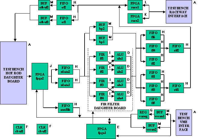
* Use the designated letters in Table 5- 1 to match board components with VHDL model
File
Use
SLOC
Figure 5- 5
Locator
dataio_loop_tb.vhd
Testbench
1515 A dataio_board.vhd
Data I/O structural
543 B firboard.vhd
FIR board structural
95 C aluchip.vhd
L4C381 entity/arch.
60 D control_fpga.vhd
Control FPGA entity/arch.
559 E cy7b991.vhd
Clock Buffer entity/arch.
39 F fct16374.vhd
16-bit Register entity/arch.
28 G fifo18.vhd
x18 SYNC FIFO entity/arch.
165 H firchip.vhd
FIR Chip entity/arch.
147 I hotrod_fpga.vhd
Hot Rod FPGA entity/arch.
924 J rino_ctl.vhd
RACEway Control FPGA entity/arch.
740 K rino_dp.vhd
RACEway Data FPGA entity/arch.
484 L sn74abt18245a.vhd
18-bit Transceiver entity/arch.
45 M
Total
5344
5.2.2 Detailed Board Design Process
The detailed, behavioral, virtual prototype was used as the specification input to the
detailed design and layout of the Data I/O board. The virtual prototype was updated as the
detailed design progressed and components were selected, so the prototype always
reflected the actual board layouts.
5.2.3 FPGA Design Process
The RASSP methodologies of virtual prototyping and a common, hierarchical, design
language were applied to the design of the two new FPGAs on the Data I/O board: Control
FPGA and Hot Rod FPGA. Each were defined in synthesizable VHDL that was used as
input to the synthesis tools and as the FPGA description in the detailed, behavioral, virtual
prototype. The FPGA I/O's signal-timing requirements were obtained from an analysis
based on the timing characteristics of the devices that interface with the FPGAs. Functional
and timing verification of the two FPGA designs were via simulation in the Data I/O
board's detailed, behavioral, virtual prototype. A separate testbench was not developed for
each FPGA. The FPGAs were exercised through the various operational modes by the Data
I/O board's testbench. This verified that the FPGAs, as defined by the VHDL code, would
satisfy functional and timing requirements.
5.2.4 Fabricate and Assemble Module
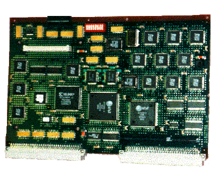
The Data I/O board (Figure 5-6) was fabricated, and the components were surface mounted
except for the FPGA's EPROMs. Socketing the EPROMs for the first physical prototype
made it easy to modify the FPGAs.
5.3 Lessons learned in Detailed Design
During the SAR processor's detailed design, a detailed, behavioral, virtual prototype was
developed for the Data I/O board, two PCB boards were designed and fabricated, and two
new FPGA designs were developed. The following are lessons learned during the detailed
design process:
![]()
![]()
![]()
![]()
Next: 6 Integration and Test
Up: Case Studies Index
Previous:4 Architecture Design