Next: 7 Conclusion Up: Case Study Index Previous:5 Detailed Design
![]()
![]()
![]()
![]()
Next: 7 Conclusion
Up: Case Study Index
Previous:5 Detailed Design
The first assembled Data I/O board was taken directly to integration and test without initial
hardware testing. The number of assembly and design problems found on the Data I/O
board were minimal (Ref. section 6.2). No defect, either in design or in assembly was
found in the Finite Impulse Response (FIR) filter's daughter card. The overall hardware
integration and test took two weeks. The hardware/software integration and acceptance test
took four weeks.
The FIR filter daughter card worked correctly the first time and required no modification.
Several problems were found on the Data I/O board during test and integration. The first
defect found and fixed was an incomplete soldering of one of the Integrated Circuits (ICs)
to the board. The remaining hardware defects related to the design of the Data I/O module
(Table 6- 1). Table 6- 2 lists the software defects and actions taken.
The test and integration of the Data I/O module were performed in several steps:
The Data I/O detailed, behavioral, virtual prototype was used during the test and integration
phase. Once a hardware problem was detected, the problem was duplicated in the virtual
prototype. The next step was to implement the fix on the virtual prototype and rerun the
suite of simulations. The impact of the fix on the SAR was determined before the fix was
made to the hardware, thereby avoiding a series of hardware modifications. These
modifications and simulations took under a day.
The data source/sink hardware proved to be somewhat fragile. Problems encountered
during test were often traced to the data source/sink, rather than to the SAR processor.
Several boards in the data source/sink had to be replaced, and it was necessary to reseat
components on the data source/sink boards every few days.
6.0 Integration and Test
6.1 Integration and Test Process Description
The final stage of the benchmark was integration and test of application software on final
hardware. The Rapid Prototyping of Application-Specific Signal Processor (RASSP)
process objective was to reduce integration and test time by eliminating defects earlier in the
design by using virtual prototyping and hardware/software co-design.
6.2 Integration and Test
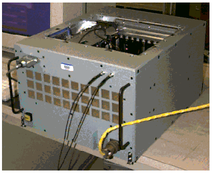
The Data I/O module was tested in the Synthetic Aperture Radar (SAR) processor's chassis
(Figure 6-1) using the real-time data source/sink hardware provided by Massachusetts
Institute of Technology's Lincoln Laboratory (MIT/LL). The Data I/O board was designed
for ease of system debug, with a bypass around the FIR daughter card and provisions for
loop-back tests using the source and sink of the Data source/sink.
Defect
Fix
Discussion FPGA reset
(logic error)
Modify one line
of VHDL code and respin
FPGA.
Testbench did not test the condition that
caused the problem. Once seen in the hardware, the
condition was duplicated in the Data I/O virtual
prototype. Two incorrect
connections on RINO
FPGA
One wire added
to Data I/O PCB.
Documentation was unclear. The model in
the detailed, behavioral, virtual prototype was
derived from the documentation. Synthesis tool
failed to implement FPGA
registers with set/reset
unspecified.
Specify
set/reset on all registers and
respin the FPGA.
Problem would have been detected
earlier if there had been back-annotation of the FPGA
implementation into the Data I/O's detailed,
behavioral, virtual prototype. FPGA layout tool
failed to implement all the
FPGA logic.
Modify VHDL
code, resynthesize, manual
modification of FPGA layout.
Problem would have been detected
earlier if there had been back-annotation of FPGA
implementation into the Data I/O's detailed,
behavioral, virtual prototype. Incorrect polarity
on Hot Rod loop-back
control
Redefined in the
firmware.
Hot Rod Fiber-optic interface was not
included in the detailed, behavioral model of Data I/O
module.
Defect
Fix Illegal transition mode from Run/Stop
Altered state transition diagram in CADRE
and regenerated code. Occasional miss of pulse on digital signal
processor (DSP)
Shut off MC/OS interference. Bad image
Pointers to old and new buffers in corner-
turn memory were swapped. Reliable start-up of all DSP processors
Incorporated system semaphores into
sequential start-up process. Caching delay on DSP
Delayed processing input of single pulses
by buffering input. Timeline problem
Corrected manually-generated code for
rubber banding on input buffer. Last image frame was not completely put out to
disk from data source/sink.
Had SAR processor put out additional data
to flush out data source/sink buffers. Crashing from memory leak in the Graphical
User Inter-face (GUI) that controlled data source/sink
from MIT/LL.
No fix; workaround was to reboot the
computer in the real-time data source-sink.
6.3 Documentation Update
The Data I/O Board Hardware Description and Operation document was updated
following integration and test. Most of the updates were added information that was not
provided in the original version but that was found to be useful during test and integration.
6.4 Acceptance Test
The acceptance test of the SAR processor occurred at Lockheed Martin Advanced
Technology Laboratories (LM ATL). Representatives from MIT/LL and the U.S. Army
attended. The first-pass design of the SAR processor successfully met all the design and
performance specifications. For budgetary reasons, the project and the Acceptance Test were descoped to include only one channel. Thus the three channel perfomance criteria was never demonstrated.
6.5 Lessons Learned in Integration and Test
6.5.1 Virtual Prototype
The following are lessons learned during integration and test:
6.5.2 Design for Testability
Features that enhanced testability needed to be incorporated into signal processor designs.
The Data I/O board's design had several features that were not required for SAR operation
but that proved very useful during test and integration. The following are those features:
6.5.3 Test and Integration Environment
Verify specialized test equipment before integration and test. For the SAR processor, real-
time testing was performed using a piece of specialized test equipment called the Data
Source/sink, which was provided by the government. The source/sink was designed and
built for the express purpose of supplying data to the SAR processor and capturing the
SAR processor's output for comparison with correct output image. Two major deficiencies
were found in the source/sink that slowed test and integration:
![]()
![]()
![]()
![]()
Next: 7 Conclusion
Up: Case Study Index
Previous:5 Detailed Design