Next: 5 Detailed Design Up: Case Studies Index Previous:3 System Design
![]()
![]()
![]()
![]()
Next: 5 Detailed Design
Up: Case Studies Index
Previous:3 System Design
The RASSP program intended to automate these four areas as much as possible. This was
accomplished by using a graph-based programming approach that supported
correct-by-construction algorithm development. The scheduling,
communications, and execution software was generated efficiently from an autocoding tool
after the user defined the partitioning and mapping of the data-flow graph onto the
specific hardware architecture. The command program was graphically captured in a state
diagram and the software code was auto-generated from the tool. An Application
Interface Builder automatically generates the application-specific interface from the
data flow graph and state
diagrams.
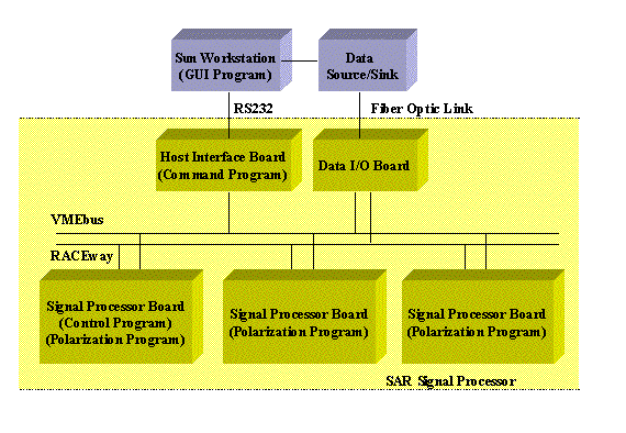
Figure 4- 2 is the SAR signal processing block diagram. The SAR Signal Processor
had to process up to three of four possible polarizations. Its architecture had to be scalable
by a factor of two in processing power and inter- processor communication bandwidth
. This scalability was for future enhancements, such as polarimetric whitening
filtering, CFAR target recognition processing, and autofocussing for other modes of
operation, such as spotlight.
Each image frame was composed of 512 pulses with 2048 complex samples per pulse.
Storing one image frame of one polarization required 8.4 Mbytes of memory, assuming 8
bytes for each complex point in the array. Azimuth
processing required two frames of data.
At the maximum pulse frequency (PRF) of 556 Hz, the 512 pulses needed to form an
image frame were collected in less then 0.92 seconds. If images for three different
polarizations were produced at this rate, then the output interface
had to support an average transfer rate of 27.32 Mbytes/sec, or 512 pulses x 2048 samples
per pulse x 8 bytes per sample x 3 polarizations x 1/.92 pulses
per second.
The interconnect bandwidth requirements were analyzed for the candidate architectures by
the performance modeling
effort.
Latency through the SAR Signal Processor could not exceed 3 seconds. The PRF of 200 to
556 pulses per second, coupled with the 512 pulses per frame, gave an interval of 2.56
seconds to 0.92 seconds between frames of the same
polarization. The three polarization frames were received interlaced, and the frame output
was required to be sequential. Latency in this case was defined as the interval between the
arrival of the last pulse of an image frame and
the start of the resulting image frame output. With this definition of latency, maximum
latency was not a design driver. Reduction of memory demand was more of a design driver
than latency when developing an implementation
that needed to process and output data as quickly as possible.
Table 4- 1 lists the memory requirements and processing throughput estimates at the
maximum input data rate and are the result of manual calculations. This provided a starting
point for the performance modeling effort that defined the
number of processors needed to meet the real-time algorithm requirements. The
48-tap Finite Impulse Response filter (FIR) and Fast Fourier Transform (FFTs) in
range and azimuth compression dominated the
processing requirement.
The memory requirements for azimuth compression were caused by corner turning.
4 Architecture Design
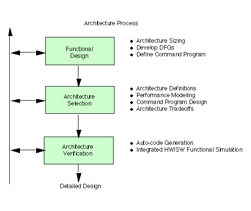
4.1 Architecture Process Description
The architecture process (Figure 4- 1) transformed processing requirements into
candidate architectures of hardware and
software elements. The system-level processing requirements were allocated to
hardware and/or software functions.
The architecture process resulted in an abstract behavioral description of the hardware and
definition of the software
required for each processor in the system. Hardware/software co-simulation verified
the correctness and performance of
the resulting architecture.
4.1.1 RASSP Innovations in the Architecture Design
Process
4.1.1.1 Hierarchical simulation (Performance Modeling)
A hierarchical VHSIC Hardware Description Language (VHDL)-based virtual
prototype approach was used for
signal-processor simulation in Rapid Prototyping of
Application-Specific Signal Processors (RASSP) methodology.
This enabled design aspects to be followed through the design process from the
Performance Model to detailed
design level within a common framework. The purposes of the performance simulations
were the following:
4.1.1.2 Autocoding Software
The software development of the RASSP architecture process deviated significantly from
traditional (functional
decomposition) approaches. The partitioned software functionality was broken into four
major areas for real-time
application software:
4.2 Functional Design
4.2.1 Architecture Sizing of SAR Algorithm
4.2.1.1 Algorithm Implementation Analysis (Latency,
Bandwidth, Computational, and Memory Requirements)

| MOPS | KBYTES | |
| Data Preparation | 33 | 49 |
| Video To Baseband (48 tap FIR) | 639 | 49 |
| Equalization | 21 | 49 |
| Range FFT | 188 | 49 |
| RCS Compensation | 7 | 16 |
| Azimuth FFT | 342 | 50,356 |
| Kernel Multiply | 41 | 254 |
| Azimuth IFFT | 342 | 254 |
| Input/Output Formatting | 16 | 25,165 |
| TOTAL | 1629 | 76,241 |
Scalability, performance, and future upgradability requirements led to the investigation of commercial-off-the-shelf (COTS), floating-point, digital-signal-processor (DSP) modules for most of the SAR processing. The FIR filter, comprising 40 percent of the total processing requirement, was a strong candidate for dedicated hardware implementation. Specialized processors sacrificed total programmability for improved efficiency in implementing a given functionality. For example, a custom module using specialized, programmable, FIR-filter integrated circuits had a recurring cost of < $2,000 to filter the processing of the SAR algorithm. If the 48-tap FIR filter processing was computed in the time domain using quad i860 COTS DSP modules, at ~$30,000 and 320 MOPS computing capability each, then the cost would have been ~$60,000. The architecture options to be investigated were identified at this point in the architecture process. The final selection was not made until after the more detailed evaluation by performance modeling and cost analysis. The detailed analysis evaluated a variety of architectures with different combinations of COTS and dedicated hardware. This included evaluation of a custom processor architecture specialized for high performance, fixed-point, block-oriented algorithms and array processing, such as FFTs.
All combinations met requirements; however, developers decided that alternative 2 was too
close to the requirement
particularly when the supplied image did not have the maximum allowed differences in
pixel values.
The following software features were common to all candidate architectures of the SAR
Signal Processor (Figure 4- 4): For a standard set of signal-processing PGM primitives developed for
the Navy: ECOS Primitives
Specification Library, CDRL Q003 and are referred to as the Q003 Primitives.
For data flow graphs and autocoding process, see the application note Autocoding for
DSP Algorithm (PGM).
The JRS RSS CAD (computer-aided design) tools were used to construct the SAR
DFG. For more information on
the CAD toolset, see Reusable Software
Subsystem (RSS) User's Manual,
JRS Research
Laboratories, March 1994. When constructing the DFG, components from the existing
library should be used. For PGM, this requires familiarity with the Q003 primitive library.
Most signal-processing functions can be implemented by using a combination of these
primitives. For the SAR, all required functions were defined down to existing Q003 library
elements. If existing primitives could not implement some of the processing, than a special
primitive would be written. The new primitives were defined within an Ada environment;
however, the underlying code for the primitive itself could be written using C language.
Also the necessary interfaces to the Autocode toolset must be generated.
A data flow graph is relatively simple to read and put together; however, it is helpful to
know the following PGM terminology. A graph represents a complete algorithm for a
particular application, such as SAR. Graphs may contain subgraphs, which provide a
particular hierarchical structure and simplify the creation of complex graphs.
An example of subgraphs are the range and azimuth subgraphs in the SAR graph ( Figure
4- 5). A graph consists of a set of nodes that represent primitive functions, such
as a Q003 library element. A node contains input and output ports (Figure 4- 6).
Queues provide the primary data storage and transfer mechanism in a PGM graph and
are represented by a first-in-first-out (FIFO) data structure. Nodes are
low-level functions that range from simple to complex and perform processing for
an application domain. An example of a node is the Finite Impulse Response (FIR) filter
(Figure 4- 7) of the range subgraph. Associated with each node was a set of Node
Execution Parameters (NEP):
The PGM provided two additional data sources: Graph Variables and Graph Instantiation
Parameters. These are individual data items and are used to parameterize the graph
during execution, such as number of taps to use in a FIR Filter or to put in the FIR
coefficients in the range subgraph.
The fundamental rule governing node execution is that a node executes when all of its
input queues contain more data then the threshold amounts. There is no notion of
sequential execution time for a node, as would occur in a conventional thread control flow.
Instead, nodes execute whenever there was sufficient data to process.
The last PGM concept to discuss is a family of nodes. Family notation allows a set of
nodes that accomplish the same function to be grouped and handled graphically as one
entity; this is, represented by a heavy outline of the box as seen by the range node and input
and output queues of range in Figure 4- 5. Families are used to simplify the
representation of parallelized functions.
The SAR algorithm has inherent parallelisms. For example, in range compression, each
pulse of data could be processed independently, so pulse data could be divided among a set
of processing nodes for concurrent processing. The SAR algorithm input signal consisted
of 512 pulses of 4064 data items. The input data stream could be split: The first pulse of
range data was sent to the first of a family of range subgraphs, and each subsequent pulse
was sent to the next family member of range subgraphs. This range processing was
grouped into one sub-graph called range (Figure 4- 7). For the SAR, this was
done in the SPLIT node using the Q003 DFC_SWTH primitive. After each data
pulse or block was processed in range, the processed data blocks were written into a
double indexed queue.
The azimuth processing could now be processed in parallel. Figure 4- 8 shows
azimuth processing, and this subgraph was called azimuth. The data was recombined with
the CONCAT node using Q003 DFC_CAT primitive to produce the full frame of
polarization data.
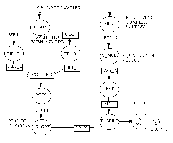
Each pulse or set of data was processed through a series of range-processing
algorithms represented by the blocks video-to-baseband, equalization weight,
range DFT, and RCS (Radar Cross-Section) calibration shown in Figure 4- 2.
The D_MUX node used the Q003 DFC_DMUX primitive to form sequences of even and
odd pulse samples. Each sequence was passed through a FIR node that had a NEP
threshold amount of 2032 and that used the Q003 FIR_R1S primitive. The node had 8 to
48 taps determined by a graph variable. The coefficients for the FIR were graph variables
to the node. Even /odd outputs were combined into a family and muxed together back into a
stream of data. The data was then converted to complex data and filled to 2048 to become
multiple of twos. The complex equalization weights, graph variables in the V_MULT node,
were multiplied with the data. Weighted I/Q data were transformed to (compressed) range
data by using a 2048-point FFT node. The FFT node used the Q003 FFT_CC
primitive. The RCS weights, graph variables in the R_MULT node using the Q003
VCC_VMULT primitive, were multiplied with the data. The FANOUT node, using the
Q003 DFC_SEP primitive, distributed the data to the appropriate azimuth channel.
Figure 4- 8 shows azimuth processing. Each range subgraph outputted segments of
range data into the number of azimuth segments. Each azimuth subgraph used the Q003
primitive DFC_SEP to collect all of the range segments that belonged in this azimuth
segment. Azimuth processing then transposed the data using the Q003 primitive
MOC_TPSE.
Developers used PGSE to simulated and debug the SAR graph. The PGSE tool provided
capabilities to execute graphs
and debug facilities that used the Telesoft Ada debugger.
The driver procedure performed the following functions:
Developers experienced difficulty with the immature and unsupported OOA2ADA tool; the
resultant code had to be extensively rewritten. There were 3500 lines of code in the
Command Program, of which 1800 were autocoded.
The CP_Callable Interface library implemented the interface between the command program
and the autocoded application software. The design of the interface library was based on
the SAR implementation in PGSE. The message structure was taken from an Auotcode Design
Document written by the autocoder vendor Management Communications and Control
Incorporated (MCCI). There were 2300 lines of code in the CP_Callable Interface.
The high throughput requirement and the accuracy and scalability requirements narrowed
candidate DSP components for the Signal Processor Boards to high-performance
floating-point processors, such as Intel's I860, Analog Devices'
ADSP21060 (SHARC), Motorola's DSP96002, and TMS320C40.T ADSP21060 had
the best performance and the I860 had the second best performance. The ADSP21060
could also cluster several DSPs together and had its own internal memory to reduce the
number of peripheral components. This allowed more DSPs per board, or about two to
three times the number of i860s.
Candidate COTS board solutions needed to be expandable to a number of DSPs across
multiple Processing Boards. Also important was the available interprocessor
communication, operating system (OS), and software support. COTS boards from
Mercury Computer Systems, Inc., were selected over comparable boards from Sky
Computer and CSPI because RASSP's autocoding tools from MCCI were being
implemented first on Mercury software.
One architecture evaluated for the SAR processor was a custom board based on the
SHARP LH9124 DSP chip. The LH9124 was a high-performance, fixed-point
DSP optimized for block-oriented algorithms and array processing, including FIR and
FFT operations. For example, the LH9124 was capable of performing a 1K complex FFT
in 80.7 microseconds, which was well under the 460 microseconds required for the Analog
Devices SHARC DSP. The LH9124 had no address capability, so it needed external
addressing, such as that generated by the SHARP LH9320 DSP address generator chip. A
signal processing board would have required a more general purpose processor for
control and system interface functions or have been managed completely by hardware
control through using FPGAs (Field Programmable Gate Arrays) .
Performance modeling and Matlab simulations were used to size the different architectures.
The eight candidate SAR processor architectures evaluated were the following:
Performance modeling goals were realized by developing VHDL token-based
Performance Models for the candidate
architectures. The Performance Models described the SAR processor's
time-related aspects, including response ,
throughput, and use. Neither the actual application data nor the transforms on it were
described, other than what was
required to control the sequence of events. For more detail on performance modeling, see
the application note Token-based Performance Modeling.
During simulation the computation agent read pseudo-code that represented the
program being executed from a file.
The four basic pseudo-code instructions were compute, send, receive, and jump. The
compute instruction represented
execution of an application subroutine as a simple time delay. The delay times were
obtained from published times
for the candidate COTS library functions. The send instruction caused the computation
agent to direct the communications agent to send a token to another CE. The token defined
the data source,
data destination, and data
packet size. The receive instruction consumed received data. If the data had arrived, the
specified queue was
decremented. If the data had not arrived, the computation agent was blocked until the data
arrived. The model tracked
how much data was stored in the various queues, but it did not store actual data.
The communications agent transferred data tokens between the local CE's memory
queues and other CEs. In the
SAR Performance Model, the communication agent broke data packets into the actual
packets that were sent over
RACEway. Upon receiving a token, the communications agent incremented the amount of
data in the appropriate
queue by the received amount. When sending a token, the agent decremented the
appropriate data queue by the
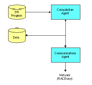
transmitted amount. Figure 4- 12 shows the top level of the computation element in
the form of the VHDL model.
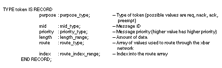
The message token used to model messages passing through the switch element was
defined as a record in VHDL
(Figure 4- 14)
The token "purpose" was used to request an interconnect link, acknowledge granting of a
request, not acknowledge
granting a request, or to preempt a link. The "route" and "index" fields were used to
determine the switch output port,
and the "length" field determined how long the link would be busy. The combination of
switch models and tokens
provided accurate modeling of the SAR processor RACEway interconnect.
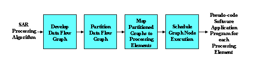
Because a single processor could not perform all SAR processing in real time, the next step
was to partition the data
flow graph into a set of partitioned graphs. The partitioned graphs were then mapped to the
processing elements in
the hardware model. Graph partitioning and mapping for the SAR application were
performed manually because tools
for automatic partitioning and mapping were unavailable.
The final step was to generate the pseudo-code application program for each
processing element by scheduling graph-
node execution. An existing program was then used to generate the set of pseudo-code
application programs for each
processing element in the SAR processor. Static partitioning/mapping/scheduling were
used because the required
processing did not change dynamically. The pseudo-code programs were stored in
files, and each instantiated
processor element in the model read its program from file during simulation and performed
the indicated operation.
Arithmetic operations were modeled by a delay, and I/O operations were used to set up the
queues in the processor
element model's communication interface.
Data communication was modeled by passing tokens through the modeled interconnect
network. The Performance Model tokens identified message type, size, source, and
destination. The size determined how long interconnect links were "busy" with the
message, and the message type was used by the receiving processing node to determine
when to fire the next processing step. When modeling the RACEway interconnect, the
tokens also included the network routing information and, in some cases, message priority.
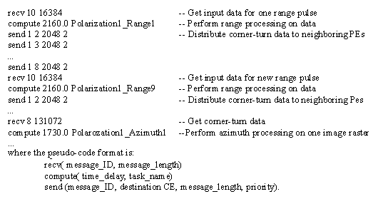
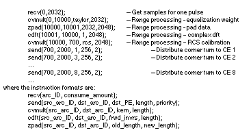
Figure 4- 16 is an example of the pseudo-code generated for a CE in an
8-CE partition by the software generation program.
Five frames of data were processed to allow processing to reach the steady-state
condition. The maximum resource requirement occurred in steady-state when data
input, range processing, azimuth processing, and data output were all active. The
performance simulations determined that three processing boards were required for the
SHARC COTS architecture and six boards were required for the i860 COTS architecture.
If the rest of the board architecture was left unaffected, then switching among SHARC or
i860 required changing only delay values assigned to processing operations in the
processing element model. This was possible because the SHARC links were not used by
the SAR processor architectures and so they were not included in the model. The full
custom SHARP-based architectures were not performance modeled, and they were
eliminated based on cost and schedule risks. A performance simulation of the
SHARP-based architectures would have required more extensive model modifications.
Also, modeling custom architectures required more effort in determining the time required
for performing standard signal-processing operations. These times were usually
available for COTS DSP boards and were incorporated into the processor element model.
Performance Model simulations also provided memory use at each processing element. The
candidate COTS architectures had memory associated with each processor element instead
of global memory. Dynamic memory use was captured during simulation by statements
included in each processor element model, and memory use was plotted after
post-processing the use data. Equalization of memory requirements over the processor
elements was desired to minimize the number of processor/memory module types. The
highest memory requirements were for the I/O control processor. This processor was a
processor element assigned the data I/O control function during mapping of the SAR
application. The performance simulations were used in developing a mapping that reduced
the I/O processor memory requirements to those of a standard module type. In addition, the
performance simulations were used to develop a priority scheme that avoided bottlenecks at
the interface to the Data I/O Board. Incoming data was given higher priority than outgoing
data.
Time-line plots of interconnect network were used to identify bottlenecks due to
hardware or software. One result of the performance-based simulations was the
determination that corner-turn data should be distributed as soon as it was calculated
during range processing. Waiting to distribute the data until a full frame of range
processing completed resulted in degraded performance due to high peak demand on the
interconnect network. The corner-turn problem was detected when the use
time-line plots for processor and interconnect link were examined. When the
corner-turn data was not distributed when first calculated, all processors were stalled
during corner-turn, while the interconnect became bogged down with multiple
corner-turn transfers at the end of each frame of range processing. When the
distribution of corner-turn data was spread over time, the number of processors
required was reduced because processors did not stall waiting for input data, and the load
on the interconnect network was leveled.
The development time for the SAR processor's VHDL performance models and
simulations took two engineers about five weeks. The total time was 371 hours. About
1378 source lines of code (SLOC) were generated for the models, and an additional 1657
SLOC were generated for the test benches that verified the correctness of the models.
Future efforts should require much less time because this original effort included significant
learning time and time to develop models from scratch. Later efforts can reuse existing
models, which will greatly reduce development time.
A SPARC- 10 CPU took 28 minutes to run a SAR processor performance simulation
of a 24-processor architecture that ran five seconds of SAR application. When
considering the number of processor elements modeled and their instruction rate, the
effective execution rate of the simulation was about 2.8 million
instructions-per-second. The performance simulations yielded measurements of
processing and communication latencies; throughput; event timelines; and use of memories,
processors, and links. The final SAR processor system met requirements with timing and
resource use, and performance fell within eight percent of that predicted by the performance
modeling.
Time-line information was captured by placing statements in the models to write the
time and name of relevant events to a history file. The history files were used to produce
time-line graphs that showed the history of task execution on each processor node.
The time-lines were useful in visualizing and understanding the impact of software
mapping options. The time-line graphs showed the time when the processor elements
were idle due to data starvation or buffer saturation, and they helped to isolate resource
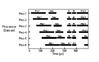
contentions and bottlenecks. Figure 4- 17 is a processing timeline plot of when
specific processor elements were busy processing tasks. Similar timeline graphs can be
generated that show when processor elements are sending or receiving data or when
communication links are in use.
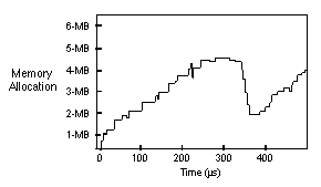
Plots of memory allocation as a function of time were valuable in visualizing and balancing
memory use during
execution of the SAR algorithm. Figure 4- 18 is a memory allocation time line from
performance modeling.
The lowest risk architecture in terms of schedule and cost was the i860 COTS Processor
Board because it was available. PRICE was used as the tool to estimate development and
life-cycle cost. The main concern with the i860 COTS boards were future
obsolescence of the i860. Intel said it did not intend to upgrade the product. However, the
i860 COTS architecture cold accommodate model-year upgrades because the
backplane interface was processor independent. The main risk associated with the
ADSP21060 COTS architecture was the availability of the COTS boards. They were
unavailable when the architecture selection decision was made. Developing a custom
ADSP21060 board or LH9124 board had greater schedule and cost risks associated with
MCM (multi-chip module) development, custom processor-board development,
and lack of software support. The final SAR processor hardware used i860 COTS boards
because of availability of the ADSP21060 COTS boards. The SAR processor architecture
provided a path for future upgrade to ADSP21060 or some other COTS boards.
The starting point for developing the SAR processor abstract Behavioral Model was the
Performance Model. The processor element models were modified by adding actual
program code for each software operation. The tokens used in modeling interconnect
network activity were augmented by the addition of a field containing the actual data in the
packet. The processor element models received the data packets, performed operations
defined by the software for the abstract application program statements, and sent data
packets to the next processing node. Sufficient memory must be allocated at each processor
element to store real data. Timing was handled using delays, as was the case for
performance modeling.
Figure 4- 19 is an example of the pseudo-code software program for the abstract
behavioral simulation that corresponds to one pulse of range processing Performance
Model pseudo-code in Section 4.3.3.2.
A comparison of this code to that for the Performance Model in Section 4.3.3.2 shows that
the two are similar, but that more information is required in the abstract Behavioral Model.
In the Performance Model all the range processing steps were lumped into one combined
delay term in a compute instruction. In the abstract Behavioral Model, each operation was
defined separately and had its own call to a procedure in the CE model.
In the Performance Model, the Data I/O Board was modeled as a source and sink for data
packets. In the abstract behavior virtual prototype, the Data I/O Board model included
functions, such as FIR filtering, that were implemented in hardware. In addition, the
abstract behavior virtual prototype was designed to interface to the Executable Specification
test bench. The Executable Specification test bench modeled the SAR processor interface at
the bit-true level, which required more detail in the Data I/O Board model to convert to
the token representation of the abstract Behavioral Model elements.
The SAR processor abstract behavioral virtual prototype was used to:
The abstract behavioral virtual prototyping required 1,171 labor hours for model
generation and simulations. The model required 3,480 lines of new code and 1,102 lines of
reuse code. Most of the reuse code was from the Executable Specification. The test benches
required 500 lines of new code and 1,657 lines of reused code.
The abstract behavioral simulation of the SAR system consumed approximately 14
CPU-hours for 5 seconds of real time data and exhibited an effective execution rate of 23,810 instructions per second. The processed output images shown in Figure 4- 20 matched the resulting target system to within - 150 dB of error power per pixel. It was much more convenient to work with smaller data sets and test images when investigating design options. A test image that was 1/64 the size of a full image was developed and used during debug.
The Autocoding Toolset was composed of the Partition Builder, MPID Generator, and the
Application Generator.
The following summarizes the development of the SAR application using the Autocoding
Toolset (Figure 4- 21):
The Autocoding Toolset produced a complete solution for the SAR application:
Autocoding demonstrated a substantial time saving as shown in Table 4- 4. Overall
development time for the real-time application software was
reduced by a factor of seven overall (10X in software development and 5 X in integration
and test time) and the development cost was decreased by a factor of 4. The processing
efficiency of the autocoded software was within 10 percent of manually optimized code.
The autocoded software data memory size was about 50 percent higher than for
manually generated code. This was a problem in testing because there was not enough
memory in the card set in the system; therefore, one of the DSP cards had to be replaced
with one that had more memory.
A new tool, LM ATL's Graphical Entry, Distributed Application Environment
(GEDAE™), corrected the above problems about one year later (See Appendix A.2).
The following were lessons learned on the command program with using an
object-oriented approach and autocoding:
4.2.1.2 Numerical Sensitivity Analysis
Matlab simulations were used to perform a numerical sensitivity analysis of the SAR
algorithm to determine if
using integer formats or fewer bits of precision would meet system accuracy requirements.
Matlab was easier and
more effective to use than was VHDL because there were available post analysis tools,
math libraries, and
experienced personnel. The reference image supplied by MIT/LL was computed using
IEEE double-precision floating
point. The SAR requirement was error power had to be less than - 103 dB relative to
maximum output signal power.
Table 4- 2 lists analysis results for the six architectures identified in Section 4.3.2 and
Table 4- 3.
SAR
Processing
Alt
1
Alt
2
Alt
3
Alt
4
Alt
5
Alt
6 FIR
SP FP
12
bit 23
bit 24-bit
BFP
12 bit
23 bit FFT
processing
SP FP
SP
FP
SP
FP
24-bit
BFP
24-bit
BFP
24-bit BFP Rest of
Algorithm
SP FP
SP
FP
SP
FP
SP
FP
SP
FP
SP FP Accuracy
- 163
dB
- 113
dB
- 161
dB
- 147
dB
- 113
dB
- 145 dB SP FP - Single Precision Floating Point
12-bit
- 12 bit integer BFP - Block Floating Point 24-bit - 24 bit integer.
4.2.1.3 First Pass Partitioning of Hardware and
Software
The following hardware features were common to all candidate architectures of the SAR
Signal Processor (Figure 4-
3):

4.2.2 Flow-Graph Generation
The SAR signal-processing algorithm was expressed using an
architecture-independent format of a Data Flow graph (DFG) implementation. This allowed Developers to
follow RASSP's
hardware/software co-design process, where the DFG algorithm could be partitioned
to hardware and software. The
SAR development used the Processing Graph Method (PGM) technology from the Naval
Research Laboratory
(NRL). This was done because PGM was a standard, at least in the Navy, and tools were
available to assist
development. See the following documents for more details:
For PGM:


4.2.3 Develop Command Program
The command program
initialized the SAR system, controlled the processing graphs as commanded by the radar
system and controlled the self-test functions. The command program was designed
using the Schalaer-Mellor object-oriented approach and the Cadre
ObjectTeam OOA/OOD tools. Information had been manually transferred from the
RDD - 100 description because RDD- 100 and the Cadre tool used different data
paradigms. The program was developed in four stages:
4.3 Architecture Selection
4.3.1 Initial Size, Weight, and Power
There was a requirement for four 6U VME customer-supplied modules to be placed in
the chassis, which led to the selection of a VME backplane for the SAR processor. The
maximum allowable dimensions for the SAR Signal Processor chassis was 10.5X 20.5X
17.5 inches, which allowed up to a 21 slot 6U VME card rack. The physical
specifications of the architecture were the following:
4.3.2 Architecture Definition
The candidate architectures included COTS and custom processor boards. However,
certain features were common to
all candidates:
4.3.3 Performance Modeling
The RASSP design process emphasized the integrated design and development of hardware
and software in a hardware/software codesign process that included performance modeling
and simulation. Performance modeling provided early design verification via simulation of
the software as partitioned, mapped, and executed on the hardware architecture. Design
verification early in the design process reduced the risk of costly architectural modifications
later
in the detailed design phase. Performance modeling enabled a range of potential
architectures to be investigated before selecting the "best" architecture for implementation
(Figure 4- 9). Performance modeling and simulation were performed during the
selection of the SAR processor architecture to help determine the size of the system,
interconnect network architecture, software-to-hardware mapping, and
performance required of each component.

4.3.3.1 Performance Modeling of the SAR Processor
Hardware
A hierarchical approach was taken to develop hardware models for performance simulation
of the candidate
architectures. Processor and switch models were at the lowest level of the hierarchy (Figure
4- 10). Tokens, rather
than actual data, represented data passing between CEs (processing elements) and through
crossbars. The token was
coded in VHDL as a record with fields that defined source CE, destination CE, data size,
data id, and route through
the RACEway interconnect.
4.3.3.1.1 CE Model
The processor element model, labeled CE in Figure 4- 10, modeled the computation
and communication of the
processor chip, such as Analog Devices SHARC or Intel i860 for the SAR processor
benchmark. Figure 4- 11 is a
block diagram of the CE model. The CE model was conceptually divided into two
concurrent processes: computation
agent and communications agent.


4.3.3.1.2 Switch Model
The switch element model, labeled X in Figure 4- 10, modeled the RACEway
crossbar when evaluating architectures
based on COTS DSP boards from Mercury Computer Systems. The Mercury crossbar had
six ports with any port
capable of connecting to any other port. Connections were made if the destination port
unblocked. The input and
output ports are shown separately in Figure 4- 13, although they were actually the
same physical bi-directional port.
Most of the switch model development time was devoted to accurately modeling how the
RACEway crossbar handled
message blocking and contention. A message was blocked if the output port was in use,
either as the output or input
port for another message. When messages arrived concurrently, priority was given to the
message that arrived on the
lower indexed port. Accurate modeling of message blocking and contention was needed to
accurately evaluate the
interconnect network performance. Once a link was established through the crossbar, it
remained in use for a period
of time determined by the data packet size. 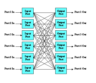
4.3.3.1.3 Hierarchical Structural Model
The CE and X elements were first assembled into models for the various board types as
shown in Figure 4- 10. The
board models were then connected together to generate the model of the entire SAR
processor. The use of the
hierarchical VHDL structural models at the processor board and system level made it easy
to modify the architecture
to investigate architectural alternatives.
4.3.3.2 Performance Modeling of the SAR Processor
Software
The first step in the process followed to develop the SAR processor software model is shown in figure 4- 5. Each graph node represented a SAR processing
primitive, such as FFT, vector
multiply, or convolution. The arcs between graph nodes represented data dependencies.
4.3.3.3 Performance Model Simulations
Several candidate SAR processor architectures were evaluated using simulation of the
VHDL Performance Model performing the SAR algorithms. For example, the number of
processing boards required was determined by simulating several image frames on models
having different numbers of boards. The simulation results were post- processed to
generate time-line plots showing use for each processing element. Changing the
number of boards required minimal effort. The structural model of the hardware was
modified by adding or subtracting boards, and the software generation program was rerun
for the different number of processors and/or mapping assignment. A change in number of
boards in the model took less than a day to complete, including resimulation. Changes to
mapping assignment were completed in four hours or less. The low-level hardware models
and the signal-processing DFGs were unchanged by the architecture variations.
4.3.4 Architecture Trade-off Analysis
The selected architecture for the SAR processor were COTS ADSP21060/2 boards with a
FIR Filter on the Data I/O Board (candidate 4 in Table 4- 3). The FIR Filter provided
greater processing margin in the COTS DSPs and a substantial recurring cost savings.
Performance Model simulations determined the processing margin. The ADSP21060
architecture was the best candidate in size and weight. Also important factors were
schedule, cost, and technical considerations. The backup architecture was the i860 COTS
Processor Board (candidate 2 in Table 4- 3).
Architecture
Candidates
1
2 (backup)
3
4 (selected)
5
6
7
8
Configuration Host I/F Module
COTS
68040 SBC
COTS
68040 SBC
COTS
68040 SBC
COTS 68040 SBC
COTS 68040
SBC
COTS
68040 SBC
COTS
68040 SBC
COTS 68040
SBC Data
I/O Module
FO I/F
TriQuint
HRC - 500
TriQuint
HRC - 500
TriQuint
HRC - 500
TriQuint HRC - 500
TriQuint HRC-
500
TriQuint HRC - 500
TriQuin
t HRC - 500
TriQuint HRC-
500
FIR
NO
PDSP16256
NO
PDSP16256
NO
PDSP1
6256
NO
PDSP16256
Complexity
Medium
High
Medium
High
Medium
High
Medium
High
Processor
Module
Type
MCV6
MCV6
MCE6/MCV6
MCV6
Custom
Custom
MC
V6
Sharp
M
CV6
Sharp
# of modules
7
5
3
2
3
2
1
3
1
3
Module Config.
4 i860's
4 i860's
8
ADSP21060
8 ADSP21060
8 ADSP21060
8
ADSP21060
4
I860
2
LH912
4
2
i860
1
LH912
4
Memory
32 Mb per
module
32 Mb per
module
32 Mb per
module
32 Mb per module
32 Mb per
module
32 Mb
per module
32Mb
26Mb
32
Mb
24Mb
Interconnect (VME +)
RACEway
RACEway
RACEway
RACEway
RACEway
RACEw
ay
RACEw
ay
RACEway
Risks Schedule/Cost
Lowest
Low
Medium
Medium
High
High
High
High Technical
Lowest
Low
Low
Low
High
High
High
Medium
Major Risk Item
Obsolescence
Data I/O
Complexity
NO VME to
MCE6
Data I/O Complexity
Software -
Board Support Package
Data
I/O Complexity
Module
Design
Data I/O
Complexity
Obsolescence
Module Availability
Module Availability
MCM Design
MCM Design
System Characteristics Recurring cost
Memory (Total System)
240 Mbytes
176 Mbytes
184 Mbytes
136 Mbytes
160 Mbytes
144
Mbytes
111
Mbytes
109
Mbytes
Computation
FFT
Single
Precision Floating Point
Single
Precision Floating Point
Single Precision
Floating Point
Single Precision Floating
Point
Single Precision
Floating Point
Single
Precision Floating
Point
24 bit
Block Floating
Point
24 bit Block
Floating Point
FIR
Single
Precision Floating Point
12 or 23 bit
integer
Single Precision
Floating Point
12 or 23 bit integer
Single Precision
Floating Point
12 or
23 bit integer
24 bit
Block Floating
Point
12 or 23 bit
integer
Accuracy
- 163dB
- 113dB (12
bits)
- 161dB (23bits)
- 163dB
- 113dB (12 bits)
- 161dB (23bits)
- 163dB
- 113dB
(12 bits)
- 161dB (23bits)
- 147dB
- 113dB (12 bits)
- 145dB (23bits) Latency
< 3 Sec
< 3 Sec
< 3 Sec
< 3 Sec
< 3 Sec
< 3 Sec
< 3 Sec
< 3 Sec Controllability, Testability, &
Maintainability
Good
Good
Good
Good
Fair
Fair
Fair
Fair
Scalability(2x)
Does not
meet requirement
Requirements met if
modify chassis design
Meets
Requirement
Exceeds Requirement
Meets
Requirement
Exceeds Requirement
Meets
Requirement
Meets
Requirement
Size & Weight
Poor
Fair
Good
Good
Good
Excellent
Good
Good
Worse Case Power (Watts)
431
371
309
299
310
300
359
320 4.4 Architecture Verification
4.4.1 Abstract Behavioral Simulation
An abstract
Behavioral Model describes function as well as timing. The model is abstract in that
interfaces are not resolved down to the individual hardware pin level. The abstract
Behavioral Model, also called the abstract behavioral virtual prototype, for the SAR
processor was generated by adding function to the Performance Model. The abstract
behavioral virtual prototype was used to verify the numerical correctness of the
software-to-hardware mapping, to generate test data, to provide system
visualization, and to verify overall SAR processor implementation. Unlike performance
modeling, actual data values were used in the abstract behavioral virtual prototype.
However, bit-true format were not necessary. Therefore, the signal links that
connected interconnect functional units were represented abstractly as pathways over which
data packets were transferred. Time resolution was at the major event level.
4.4.2 Autocode Generation
The Autocoding Toolset developed by MCCI was used to render the SAR PGM graphs
into a set of C language source files that implemented SAR's signal processing
functionality. The source code produced contained calls to the MCCI's Static Run
Time System (SRTS) libraries, which provided run-time support for graph execution
and control and for queue/data management.


Lines
of
Code
Total number of lines of code generated with autocoding was 60 percent
greater than hand-coding Performance
Same number of processors; about equal with hand-coding, within 10 percent
Memory
Amount of data memory was 50 percent greater than hand coding. This was an
impact because a DSP card with more memory was required Development
time
10X improvement over hand-coding Test time
5X improvement over hand-coding 4.5 Lessons Learned in the Architecture Design of the SAR
Benchmark
4.5.1 Hierarchical Simulation (Performance Modeling)
Creation of the SAR processor Performance Model was a learning experience for LM ATL.
Techniques and models were not in place when the benchmark started. LM ATL had
performed performance modeling effectively in the past on multiprocessor systems using a
'C-language- based in-house tool called CSIM. The lessons learned
during the performance modeling effort were the following:
4.5.2 Hierarchical Simulation (Abstract Behavioral)
Adding actual data and processing operations to the Performance Model created the abstract
Behavioral Model for the SAR processor. The resulting virtual- prototype simulations
were numerically correct for the software mapping to the hardware. The following were
lessons learned during the development of the abstract behavioral virtual prototype
development and simulation:
4.5.3 Autocoding Software
The SAR benchmark was performed early in the RASSP program before several of the
RASSP tools used for the software development were in place. The following were lessons
learned with data flow capture using the PGM based tools from JRS' PGM"
based tools and MCCI's beta version of the Autocoding Toolset:
![]()
![]()
![]()
![]()
Next: 5 Detailed Design
Up: Case Studies Index
Previous:3 System Design