Next: 3.0 ETC4ALFS on COTS Summary Up: Case Studies Index Previous:1.0 Introduction
![]()
![]()
![]()
![]()
Next: 3.0 ETC4ALFS on COTS Summary
Up: Case Studies Index
Previous:1.0 Introduction
Therefore a single FPCAP module has more processing power then the 3 AP/FE (9 cards) and more memory then the 2 GM/FE (4 cards) that are in the current AN/UYS-2A configuration scheduled for ALFS deployment on the SH-60R helicopter.
Due to the required custom form factor, a complete commercial-off-the-self (COTS) approach was not possible for the AN/UYS-2A upgrade. Instead, commercial parts were used on the custom modules, which also allowed the maximum use of commercial tools such as compilers and real time operating systems. Commercial grade components were used on the design that allowed saved over 60% of the production cost and a large amount of NRE that would have been necessary to qualify the parts. The architecture that resulted consisted of a control module (FPCTL) and two identical processor modules (FPCAP) in the basic FPCAP/FE. Adding additional FPCAP modules increases processing power.
A VHDL performance model was created for the three modules of FPCAP/FE. Performance modeling simulation of the required processing showed the architecture meeting processing, memory, and communication bandwidth requirements.
The FPCTL module design phase took only 13 weeks to complete. The design schedule for this module is >2X improvement compared to the best times achieved on similar complexity modules developed in the past at one location. The design included development of a full detailed behavior virtual prototype of the module, FPGA and PLD designs, module layout, and manufacturing data including design of assembly fixtures. This short design cycle time was achieved by a combination of virtual prototyping and concurrent engineering. The hardware and software design was spread across four companies at five different locations. This placed a premium on timely interchange of design information and requirements between all the parties involved.
The development of the VHDL based virtual prototype of the FPCTL module was an important step in the design process in several critical areas:
The virtual prototype was used to verify the design of both the hardware and software interfaces to the AN/UYS-2A legacy system and the internal interfaces within the FPCTL. This functionality verification consisted of simulating of the hardware performing low-level software operations. The detailed behavior virtual prototype also verified the operation of the FPGA and PALs designs.
The 13-week design cycle for the FPCTL module entailed concurrent design in which the virtual prototype, logic design, PCB layout, and software design proceeded in parallel. The exchange of information between the different design activities at different locations was facilitated by weekly conference calls between all parties. Preliminary versions of the hardware design and software design specifications were generated and distributed to all members of the design team for review by electronic mail. These specifications were updated at least every two weeks, and were used as the basis to decide modification to hardware and system architectures. Manufacturing engineers were brought in early in the design process to insure that the final design could be manufactured at lowest possible risk and cost. The result was a rapid turn-around of the FPCTL design with no "surprises" during module assembly, module test and system integration.
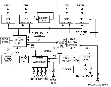
The FPCTL design shown in figure 2-1 makes use of four custom legacy ASICs of two types, the PIP/POP and the CBI/FBIT, that were designed by AT&T (now Lucent Technologies) for the AN/UYS-2A. The existing VHDL code for these two ASICs was incorporated into the detailed behavior virtual prototype. It was found that the ASIC BIST features, and several other features supporting test, were not modeled. Some additions were made to the ASIC VHDL models to provide minimal coverage of these features. The PIP/POP and CBI/FBIT ASICs are being used in a manner for which they were not designed. Using the ASIC VHDL models with the FPGA VHDL model, a new interface was developed that allowed current components to replace obsolete components. During simulation behaviors were encountered that were not anticipated from reading of the written documentation. As a result, several potential errors in interfacing to the ASICs were detected early in the design process. A big benefit from using the legacy VHDL models is the unambiguous nature of the VHDL code when compared with written documentation. Without the legacy VHDL models, insufficient information would have been available for designing the interface to the legacy ASICs without errors.
Figure 2-1 FPCTL Block Diagram
A challenging facet of FPCTL design is the interface between the various asynchronous ports, each with its own protocol. It provides all the communications interfaces to the AN/UYS-2A system buses:
As well as the communications to the FPCAP modules via the LANai, a RISC processor that provides the interface between a Myrinet link (160 Mbytes per second bandwidth in each direction) and the SHARC External Processor Bus. Myrinet data being sent or received is buffered in the high-speed 128K LANai SRAM. A 128K-by-48 SRAM that can be accessed by either the SHARC or the LANai, a 512K-by-8 flash memory that boots the SHARC at power-up, a test bus controller for JTAG test of FPCAP modules, and two independent clock oscillators with clock buffers.
To facilitate the use of the latest technology in new systems and the insertion of new technology into existing systems, RASSP defined the concept of hierarchical virtual prototyping for embedded multiprocessor systems. The virtual prototype provides the ability to simultaneously simulate the hardware/software co-design and predicts the performance of the design on the hardware architectures prior to building the hardware.
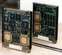
Exercising the detailed behavior virtual prototypes through the various operational modes performed design verification testing prior to hardware build. The result of the design verification was a design that met functional and performance objectives. The FPCTL board design had no redesign iterations, and only 4 white wire corrections were required on one of the two custom printed wiring boards on the SEM-E module shown in Figure 2-2. The corrections were necessary to correct problems due to a glitch out of one the legacy ASICs and fix a design error due to a late change in one of the FIFOs for board space reduction which was not adequately modified on the virtual prototype.
Figure 2-2 FPCTL Module
The FPCTL is a dense surface mount module preventing significant probing during test and integration. As a result, the virtual prototype was used to provide insight into the observed hardware operation. The virtual prototype was used to determine if hardware failure, design flaws, or simple misunderstandings were the cause of unexpected behaviors.
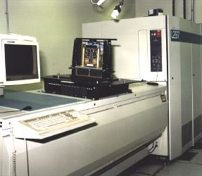
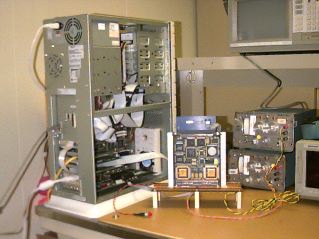
The FPCTL modules were quickly tested and debugged in 4 weeks which included verifying test programs on a Teradyne L297 Automatic Test Equipment (ATE) for manufacturing test and on a PC for field testing. This is a saving of more then a month off past designs. This 2X quicker completion of module testing was due to the design-for-test features in the hardware and software design.
Figure 2-3 Teradyne 297 FPCTL test set-up for production test
Figure 2-4 FPCTL field or depot testing with PC
Integration of the FPCTL module with the board support package software (30,000 source lines of C code), communication drivers, multiprocessor SPOX real time operating system, and debug monitor took only 2 weeks. The only problem encountered was that SHARC Link communications are more sensitive to cable length than SHARC literature indicated. This may have been a combination of many interconnection effects. The cable is only used for portions of integration and test, and is not actually part of the deliverable system. Since it was an interim problem, the cable was shortened to resolve the problem.
A similar board support package integration on the second generation APU module available from the HPSC program which was developed without HW/SW co-design and verification took over 12 weeks.
2.0 UYS-2A Signal Processor Upgrade
The program objective was to replace the existing Arithmetic Processor Functional Element (AP/FE) in the AN/UYS-2A with a Floating Point Commercial Arithmetic Processor Functional Element (FPCAP/FE), and to implement the Echo Tracking Classifier (ETC) algorithm for Airborne Low Frequency dipping Sonar (ALFS) on the upgraded hardware. A requirement for the AN/UYS-2A Upgrade was that the FPCAP/FE modules operate in the AP/FE slots of the existing chassis and interface to the rest of the AN/UYS-2A in both hardware and software. The basic FPCAP/FE consists of three SEM-E modules, the control module (FPCTL), where the hardware and software to interface to the existing UYS-2A system resides and two signal processor modules (FPCAPs), that perform the bulk of the signal processing. The state-of-the-art processing, memory, and communication bandwidth improvements of the FPCAP/FE (3 card set) beyond the current Arithmetic Processor AP/FE (3 card set) and Global Memory GM/FE (2 card set) are:
Processing Memory Bandwidth 2.1 FPCTL Module and software development
2.2 Virtual Prototype and Design-for-Test accelerated integration
2.3 Software / hardware integration reduced by 6X by use of virtual prototype.
![]()
![]()
![]()
![]()
Next: 3.0 ETC4ALFS on COTS Summary
Up: Case Studies Index
Previous:1.0 Introduction