This document provides, in matrix form, a comparison between non-scan and scan solutions, and compares LSSD and non-LSSD scan implementations. It becomes clear that scan has significant advantages over non-scan:
This document also investigates several methods of LSSD implementation for ASIC designs. The D-Mimic and Clock Splitter approaches are compared for the CMOS-4LP and CMOS-5L technologies, both for Standard Cell and Gate Array implementations. Through these comparisons, the following LSSD design recommendations become clear:
Test Coverage: Quality Measurement
Chip Area: A Hardware Overhead Measurement
Chip I/O: A Hardware Overhead Measurement
System Performance: A Hardware Overhead Measurement
Scan Performance: A Hardware Overhead Measurement
Isolation and Debugability: A Time-to-Market Measurement
Test Pattern Schedule: A Time-to-Market Measurement
Test Pattern Processing: A Cost Measurement
Test Equipment Cost: A Cost Measurement
Tester Time: A Cost Measurement
Enabled Benefits: Other Positive Factors enabled as a result of implementation of a given design structure
The following design structures are compared:
Leaf Splitter LSSD
See the Section "ASIC Scan Implementations" for a description of various Scan and LSSD approaches.
---------------------------------------------------------------------------------------------------------------------------
Factor non-Scan non-LSSD Scan LSSD Scan
---------------------------------------------------------------------------------------------------------------------------
Quality
Test Coverage 80-90% >99% >99%
Hardware Overhead
Chip Area As necessary 9% (Note 1) Leaf Splitter 7%
(Note 1) to provide D-Mimic 15%
desired Func (Note 1)
tional Test
Coverage
Chip I/O See above Scan_Mode 1 ABC Clocks 3
(Note 2) (Note 2)
System See above Mux (~300ps) <100ps
Performance in Data Path
Issues
Scan n/a Possible short None
Performance path race condi
Issues tions
Time to Market
Isolation and Weeks Days Days
Debugability
Test Pattern Months Hours Hours
Schedule
Cost
Test Pattern Days/Weeks, Hours Hours
Processing some designs
(CPU) require
hardware
accelerator
Tester Cost Test equip Enables Enables
ment must Reduced-Pin Reduced-Pin
access All Tester * Tester *
Chip Pins
Tester Time <10 seconds � <10 � <10
for 80-90% � seconds � seconds for
coverage for 80- 80-90%
90% coverage
� coverage � Tester time
� Tester increases
time for higher
increases coverage
for higher
coverage
*With Boundary Scan
Note 1: An estimate, based upon 20% of chip area used for
registers.
Note 2: Does not include SDI and SDO pins, which can be shared with
existing System I/O. There is also a capability to share the
ABC clocks pins as well, reducing the pin overhead to a sin
gle Scan_Mode input.
---------------------------------------------------------------------------------------------------------------------------
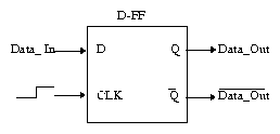
FIGURE 1: D-FlipFlop for a Non-Scan Design Structure
This section will provide qualitative comparisons between scan implementations and DFF-based non-scan implementations. The following section, "Comparisons Between ASIC Scan Implementations", will quantify these comparisons in summary form for Standard Cell and Gate Array technologies.
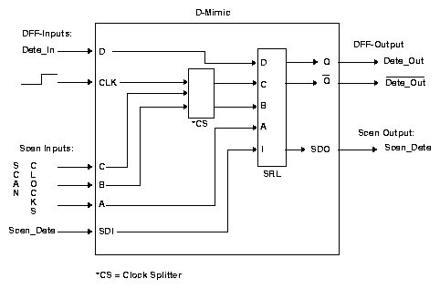
FIGURE 2: D-Mimic LSSD Design
Comparison Characteristics
Register External View
Input---D-FF with SDI and Scan Clocks A,B,C
Output---D-FF with SDO
Register Logic SRL plus Clock Splitter for D-FF compatibility
Clock Tree Full Trees for A,B,C
System Data Delay Minimal
System Clock Effect None: Splitter is local to SRL
Scan Race Exposure None: LSSD
Added Clock Pins A,B,C
Other Considerations This method is extendable to the use of Asynchronous Set/Reset Latches
through the use of the D-Mimic with Asynchronous Set/Reset SRL.
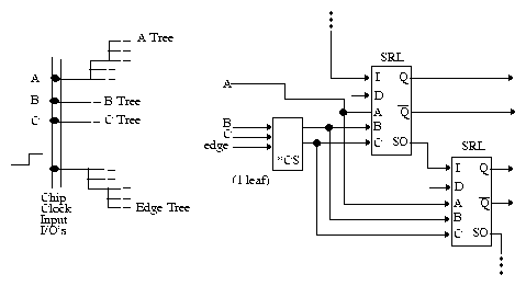
Comparison Characteristics
Register External View
Input---D-FF with SDI and Scan Clocks A,B,C
Output---D-FF with SDO
Register Logic SRL
Clock Tree Splitter at each Leaf of B,C,edge Powering Trees, full A Powering Tree
System Data Delay Minimal
System Clock Effects Minimal or None: Splitter placed after all Clock re-Powering
Scan Race Exposure None: LSSD
Added Clock Pin A,B,C
--------------------------------------------------------------------------------------------------
Circuit                                                                Standard Cell  Gate Array
--------------------------------------------------------------------------------------------------
SRL                                                                    CBLY=7         CBSS=12 ****
D-Mimic SRL                                                            CBNI=8         CBIK=15
D-FF                                                                   6*             CBVI=8
D-FF w/Mux                                                             9*             11*
Leaf Clock Splitter                                                    CBSF=12        CBH8=20
*  Circuit is not currently offered. Number shown is a projection.
****  Supporting pseudo book models not currently available. Contact
your Application Engineer for support in obtaining the option of
CMOS4LP Gate Array with Leaf Splitter LSSD.
--------------------------------------------------------------------------------------------------
TABLE 2: CMOS4LP Cell Counts (Medium Power)
Note on D-FF's: The D-FF circuits described here are hypothetical, projected for the purpose of making chip area comparisons to the scan-based approaches. As such, although the following comparisons are based upon these D-FF's, such logic circuits do not actually exist in the design libraries.
----------------------------------------------------------------------------------------------
Circuit                                 Scan      Total   System   System    Scan      Added
                                        Cell      Area    Clock    Data      Data      Pins
                                        Growth    Growth  Penalty  Penalty   Race      (beyond
                                        (S =      *                          Exposure  SDI /
                                        SRLs)                                          SDO)
----------------------------------------------------------------------------------------------
Leaf                                    1.57 x S  5%      Minimal  No        No        3
Splitter
D-                                      2.25xS    8%      No       No        No        3
Mimic
D-Mux                                   3xS       10%     No       2-Input   Yes       1
                                                                   Mux
* Based on DFF_area = 20% of chip_area
----------------------------------------------------------------------------------------------
The following diagram shows how this is done:
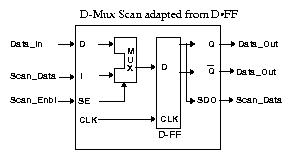
FIGURE 4: D-Mux Scan (non-LSSD Comparison)
Comparison Characteristics
Register External View
Input---D-FF with SDI and Scan_Enbl
Output---D-FF
Register Logic D-FF with Mux.
Clock Tree No additions
System Data Delay Mux Delay
System Clock Effects None
Scan Race Exposure--- Short Path Exposures exist for SDO to SDI path. Must be accounted for in the System Design.
Added Clock Pins None.
Other Considerations
Adds a Scan_Enbl pin
Scan must operate correctly at the edge clock frequency
This non-LSSD approach is not supported for IBM ASICs.
--------------------------------------------------------------------------------------------------
Circuit                                  Scan      Total     System   System    Scan      Added
                                         Cell      Area      Clock     Data     Data      Pins
                                         Growth    Growth *  Penalty  Penalty   Race      (beyond
                                         (S=SRLs)                               Exposure  SDI/
                                                                                          SDO)
--------------------------------------------------------------------------------------------------
Leaf                                     4.97xS    12%       Minimal  No        No        3
Splitter
D-                                       7.25xS    19%       No       No        No        3
Mimic
D-Mux                                    3xS       8%        No       2-Input   Yes       1
                                                                      Mux
*  Based on DFF_area = 20% of chip_area
--------------------------------------------------------------------------------------------------
---------------------------------------------------------------------------------------------
Circuit                                                             Standard Cell  Gate Array
---------------------------------------------------------------------------------------------
SRL                                                                 CHRG=9         CHHO=14
D-Mimic SRL                                                         12 *           CHJ4=17
D-FF                                                                7 *            9 *
D-FF w/Mux                                                          12 *           14 *
Leaf Clock Splitter                                                 CHQV=12        CHIJ=14
*  Circuit is not currently offered. Number shown is a projection.
---------------------------------------------------------------------------------------------
TABLE 5: CMOS5L Cell Counts (Medium Power)
Note on D-FF:
The D-FF circuits described here are hypothetical, projected for the purpose of making chip area comparisons to the scan-based approaches. As such, although the following comparisons are based upon these D-FF's, such circuits do not actually exist in the design libraries.
------------------------------------------------------------------------------------------------------
Circuit                                   Scan Cell   Total    System   System    Scan Data   Added
                                          Growth      Area     Clock    Data      Race        Pins
                                          (S=SRLs)    Growth   Penalty  Penalty   Exposure    (beyond
                                                      *                                       SDI/SDO)
------------------------------------------------------------------------------------------------------
Leaf                                      2.57xS      7%       Minimal  No        No          3
Splitter
D-Mimic                                   5.25xS      15%      No       No        No          3
D-Mux                                     5xS         14%      No       2-Input   Yes:        1
                                                                        Mux
*  Based on DFF_area = 20% of chip_area.
------------------------------------------------------------------------------------------------------
----------------------------------------------------------------------------------------------------------
Circuit                                   Scan Cell   Total Area   System   System    Scan Data   Added
                                          Growth      Growth *     Clock    Data      Race        Pins
                                          (S=SRLs)                 Penalty  Penalty   Exposure    (beyond
                                                                                                  SDI/
                                                                                                  SDO)
----------------------------------------------------------------------------------------------------------
Leaf                                      5.72xS      13%          Minimal  No        No          3
Splitter
D-Mimic                                   8.25xS      18%          No       No        No          3
D-Mux                                     5xS         11%          No       2-Input   Yes:        1
                                                                            Mux
*  Based on DFF_area = 20% of chip_area.
----------------------------------------------------------------------------------------------------------
TABLE 7: Comparison of Scan Implementations toD-FF - CMOS5L Gate Array
--------------------------------------------------------
Block  Function       LSSD Method    Technology  Library
--------------------------------------------------------
CBIK   D-FF           D-Mimic        CMOS4LP     GA
CBIL   D-FF w/        D-Mimic        CMOS4LP     GA
       Asynch S/R
CBIM   JK-FF          D-Mimic        CMOS4LP     GA
CBIN   JK-FF w/       D-Mimic        CMOS4LP     GA
       Asynch S/R
CBMG   D-FF           D-Mimic        CMOS4LP     SC
CBNI   D-FF (dense)   D-Mimic        CMOS4LP     SC
CBNJ   D-FF (dense)   D-Mimic        CMOS4LP     SC
CBTA   D-FF           Leaf Splitter  CMOS4LP     SC
CBLY   D-FF (dense)   Leaf Splitter  CMOS4LP     SC
CHJ4   D-FF           D-Mimi         CMOS5L      GA
CHH3   D-FF w/ Reset  D-Mimic        CMOS5L      GA
CHH5   D-FF w/ S/R    D-Mimic        CMOS5L      GA
CHH0   D-FF           Leaf Splitter  CMOS5L      GA
CHHP   D-FF           Leaf Splitter  CMOS5L      GA
CHRG   D-FF           Leaf Splitter  CMOS5L      SC
--------------------------------------------------------
----------------------------------------------
Block  Function            Technology  Library
----------------------------------------------
CBIA   D-Latch (2 output)  CMOS4LP     GA
CBTA   D-Latch             CMOS4LP     SC
CBLY   D-Latch (dense)     CMOS4LP     SC
CHHP   D-Latch             CMOS5L      GA
----------------------------------------------