System09 Revision Log
20th March 2003
Interim Snap Shot .
30 March 2003
Snap shot of a 6809 design as of 30th March 2003 uses 109% of slices in an XC2S200 FPGA so does not compile. It includes a 2K Monitor ROM which is probably what is taking up all the LUT's
The 6809 is currently missing the following features
1. No FIRQ
2. No SWI2 or SWI3 although it does decode those op codes
3. E Flag (Entire) does not prevent stacking of registers
I have replaced the parallel I/O port with Compact Flash support using the B5-CF module in 8 bit IDE mode
29th April 2003
It does not appear to work at this stage, although the test bench seems to indicate it should print out the "Hello World" message to the UART. Using the Hello World test ROM in place of the Boot ROM does not appear to work.
I have removed the 2K SBUG9 monitor ROM and included a 256 byte ROM which should Boot SBUG9 from Compact Flash. The 256 byte ROM is mapped at the top of memory on reset. On reset, the boot ROM should copy itself to RAM, then boot an Image of SBUG from the B5-CF Compact Flash into write only RAM at $F800 - $FFFF before switching the ROM out and making the RAM at $F800-$FFFF read only.
On reset, The ROM is mapped at $FF00 and a write to $F800 - $FFFF write to shadow RAM. By writing to location $E030, the ROM should be mapped out, and the Monitor RAM is made Read Only. A Write to $F800-$FFFF will then write to the Dynamic Address Translation registers.
The 256 byte boot ROM configures the B5-CF Compact Flash module for 8 bit LBA mode. The Boot ROM should load 4 x 512 byte sections containg SBUG at LBA Address $0F47C - $0F47F. You need to use the Compact Flash sector write routines (cf.zip) with the System68 design to write an image of SBUG to the Compact Flash.
So far as I can tell, the Compact Flash is being accessed as the activity led blinks shortly after the release of Reset. I've tried implementing the Compact Flash boot in a known working CPU design on the board (System68) but that does not work either. System68 works fine with internal ROM, but will not boot SWTBUG out of compact flash using the same boot ROM switch as the System09.
The System09 design uses 97% of Slices in an XC2S200 FPGA, so its a tight fit .... It would be good to have a B5 board with 300K gates as I could then include the SBUG ROM in the FPGA.
I've implemented FIRQ, and the E (Entire) bit, and SWI2 and SWI3 missing on the previous snapshot. One of the Test Benches should exercise all the Software Interrupts. I've also modified the PSH/PUL instructions so they only execute cycles when there is a register to be pushed or pulled.
29th June 2003
Hans Pufal has suggested that I make use of block RAM so that I can fit the SBUG monitor ROM into the FPGA with the CPU. this eliminates the need to boot the monitor ROM image from Compact Flash. So far I have not managed to get the block RAM working as a ROM. Refer to the System68 design for a further discussion on the use of block RAM. With the Slice test ROM installed the CPU spits out 13 x " ' " or 0x27 characters. This is the exact number of characters in the "Hello World\d\n" string. I can find nothing in the simulation that explains this. The CPU seems to be working fine in the behavioural simualtion, so I suspect there is a timing issue to contend with.
I have fixed a few bugs in the state sequencer with this snapshot.
19 July 2003
Prints out "Hello World"
After a bit of a break, I have got back into the 6809 design and found a bug in the MiniUART. Now it prints out "Hello World". Wooo Hoo !!!! I have been advised that NMI's should be disabled until the S Stack pointer has been set up with an LDS or LEAS. I have yet to implement that suggestion.
5 September 2003
Works with SBUG Monitor ROM
Well it appears to work .... Tony Burch has loaned me a B5_X300 which has given me enough space to include a 2 K Slice ROM. Note however that I am still using a modified B3_SRAM board and the B3_FPGA_CPU_IO module. If you are using Tony's latest B5 modules, you will have to update the User Constraint File to reflect the new pin out.
There are some issues with regard to clock edges. I thought the CPU clocked on the falling edge of the system clock but it appears, after simulating the entire system, to clock on the rising edge. I have not done it on this version, but I need to change the clock edge so that I can use alternate clock phases on the block RAM. I did manage to get System68 to read Block RAM ROM by reversing the clock edge. It appears I was gating the write on the first half of the cycle rather than the second half, which explained the problems I was having. It certainly helps to simulate the design properly.
There were a few bugs I found in the core:
-- Fixed 16 bit indexed offset, It was doing reading the offset at the EA rather than fetching it at the PC address
-- Added/Fixed STY and STS instructions - STY and STS was not decoded correctly in the second page decode state
-- ORCC_STATE ANDed CC state rather than ORed it - Now fixed
-- CMPX Loaded ACCA and ACCB - Now fixed
I've also cleaned up the component end entity syntax. The Modeltech simulator is much more fussy about synctax than the XST VHDL synthesis tools.
There are bound to be more bug fixes, so stay tuned for any updates.
6th September 2003
Initial Open Cores version
This is a screen of the version released to the open cores web site on 6th September 2003. It should be the same as the version above, except I commented the code a bit more.
16th September 2003 3:10 am AESTNow using Block RAM
I finally got the Monitor Program running in Block RAM. This version uses 81% of the slices of a XC2S300e. The version with Slice 2KByte ROM uses 3070 out of 3072 slices so it was a pretty tight fit. I thought the ROM would use more slices than it does.
Device utilization summary:
Number of External GCLKIOBs 1 out of 4 25%
Number of External IOBs 83 out of 142 58%
Number of LOCed External IOBs 83 out of 83 100%
Number of BLOCKRAMs 4 out of 16 25%
Number of SLICEs 2494 out of 3072 81%
Number of GCLKs 1 out of 4 25%
I'm now using a B5-SRAM module and the B5-Peripheral-Connectors Modules with the B5-X300 FPGA board. The B5-SRAM is installed on connectors E & F, I'm using the B5-Peripheral-Connectors on connector C and I have the B5-CF Compact Flash installed on connectors A & B. The UCF file should contain all the relevant pinouts. The Clock is Running at 9.8 MHz or so (I think) and the baud rate is 9600Bd.
--------------------------------------------------------------------------------
Constraint | Requested | Actual | Logic
| | | Levels
--------------------------------------------------------------------------------
TS_sysclk = PERIOD TIMEGRP "sysclk" 100 | 100.000ns | 56.524ns | 11
nS LOW 50.000000 % | | |
--------------------------------------------------------------------------------
TIMEGRP "ram_cs" OFFSET = OUT 40 nS AFTE | 40.000ns | 35.583ns | 14
R COMP "sysclk" | | |
--------------------------------------------------------------------------------
TIMEGRP "ram_wr" OFFSET = OUT 40 nS AFTE | 40.000ns | 31.006ns | 11
R COMP "sysclk" | | |
--------------------------------------------------------------------------------
TIMEGRP "ram_addr" OFFSET = OUT 40 nS AF | 40.000ns | 36.781ns | 13
TER COMP "sysclk" | | |
--------------------------------------------------------------------------------
TIMEGRP "ram_data" OFFSET = OUT 40 nS AF | 40.000ns | 35.755ns | 11
TER COMP "sysclk" | | |
--------------------------------------------------------------------------------
TIMEGRP "ram_data" OFFSET = IN 15 nS BEF | 15.000ns | 12.610ns | 5
ORE COMP "sysclk" | | |
--------------------------------------------------------------------------------
TIMEGRP "test_alu" OFFSET = OUT 90 nS AF | 90.000ns | 55.967ns | 22
TER COMP "sysclk" | | |
--------------------------------------------------------------------------------
TIMEGRP "test_cc" OFFSET = OUT 95 nS AFT | 95.000ns | 63.168ns | 24
ER COMP "sysclk" | | |
--------------------------------------------------------------------------------
| 50ns | 50ns |
SysClk -----\___________________/--------------------\________ (10MHz)
| 37ns |
ram_addr ----------------<==================================>---
| tacc = 50ns > 15ns | 13ns |
ram_data --------------------------------------<==========>---- (read)
The conclusion is, you could probably shave 20nsec off the cycle time and it would still work reliably. ie. should run at 12.5 MHz. It would depend on the required set up time of the block RAM which clocks the address and data on the rising clock edge.
29th November 2003 release B.
This version corrects some errors in indexed addressing. ACCA and ACCB indexed offset should be 2's complement. I have now sign extended them in the Right ALU mux. Also absolute indirect addressing had an error in the bus cycle for for picking up the low byte of the 16 bit absolute address. It performed a read rather than a fetch cycle. It has now been fixed.
The errors were picked up by a more comprehensive test of addressing modes, using TESTBENCH5.VHD. I can now execute a SWI in a program and CPU09 will return to the monitor program correctly.
29nov03b fixes up the problem with breakpoints. I assumed the LEA instructions did not affect the condition codes. In fact LEAX and LEAY affect the Z flag. LEAS and LEAU do not affect any condition code flags. SBUG relied on an LEAY -3,Y to clear the Z Flag. I've added an extra ALU control function "alu_lea" which does the same thing as the "alu_ld16" (16 bit load) but only affects the Z condition code.
It was also suggested to me sometime back that interrupts should be disabled until the S stack pointer is loaded either with an LDS or LEAS instruction. I have still yet to do that.
I'm now using WebPack ISE 6.1. They have made a number of changes, and now I am not sure what they have done with the User Constraint File.
12th December 2003
Fix on CWAI. Microcode did not push the return state before masking the Condition Codes - Thanks to Ghassan Kraidy for picking up this fault.
17 January 2004
CLR fix, Updated UART.
The CLR instruction did not clear the carry flag. This was picked up by Michael Hasenfratz. It affected a number of CPUs in the SystemXX range. It was due to an error in the ALU control in the state sequencer.
I've also updated the miniUART so that it supports synchronous X1 clock inputs. I've also added CTS control of the transmitter and DCD interrupts and receiver control.
I've updated the start bit synchroniser in the UART. There was a race condition on the start bit level detect and edge detect that resulted in unreliable operation. The UART now works reliably at 38.4 Kbaud.
26 January 2004
Numerous bug fixed
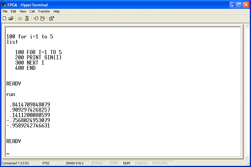
After an all night session I have XBASIC running on System09.
Bugs found are as follows:
1. PSHU was referencing the SP in one of the states
2. STD instruction did not set the condition codes
3. JMP direct was not implemented
4. CLR direct performed an addition read cycle which was not necessary
5. Bogus latch instruction prevented page2 indexed instructions from working
6. Minor alterations to microcode subroutine calls.
7. removed "test_alu" and "test_cc" signals to free up I/O ports.
8. TFR did some strange things to the condition codes, although should not have had any harmful effects
9. removed redundant "alu_inx" and "alu_dex" definitions
S1 Dump of Flex9
S1 Dump of XBasic
System09 runs at 38K4 baud with a 4.9 MHz (9.8 MHz ???) clock. (8 data 1 stop bit)
On reset you should get the SBUG message and a ">" prompt
Put SBUG in load S1 Load mode by pressing the "L" key
Send the F9.s19 file with Hyperterm in text download mode. (no handshake protocol is used)
Set the PC to $CD00 (<ctrl> P CD00)
Execute Flex by pressing the "G" key
Enter the date and you should get a +++ prompt
Return to SBUG by entering "MON" <enter>
Put SBUG in load S1 Load mode by pressing the "L" key
Send the XBASIC.s19 file with Hyperterm in text download mode.
Set the PC to $0000 (<ctrl> P 0000)
execute XBASIC by pressing the "G" key
Type in a basic program.
Screen dump of XBASIC running under Flex9 (only runs console I/O at this stage)
1 February 2004
Runs Flex9 Operating System
Two basic bugs:
1. CWAI did not increment the program counter in one of the bus cycles
2. ABX was performing a signed addition rather than unsigned like it should have
I have added Bus trap logic that allows an NMI to be generated on any address, any data and any read/write and vma condition. this hardware is useful for trapping writes to specific memory locations. There is no documentation on it yet, so you will have to read the header of the VHD file to find out how it works.
I have written a RAM disk driver that uses the DAT and the top 192K bytes of RAM. It requires a disk geometry of 48 tracks x 16 sectors per track. I have used the Evenson SWTPC emulator and floppy disk maintenance tool to generate the required disk format. I used a "makehex" utility written in C to convert the binary disk image into a ASCII hexadecimal dump. I have written a RAM disk download utility for the 6809 called "ramdskdl" and I have overlayed my ram disk drivers on a binary copy of Flex9.
Flex9sys.zip - Disk images, RAM disk downloader and Flex9 binary
The procedure is as follows:
Download the Flex9.s19 binary image using the SBUG "L" command
Download the Ramdskdl.s19 binary image using the SBUG "L" command
Set the program counter to $1000 (<ctrl> P 1000)
Execute the program with the "G" key.
Ramdskdl will prompt you to download the disk image
Being careful not to press any keys on hyperterm, send the Flex hexidecimal disk image "flex9sys.hex" as a text file. This will take a few minutes. The file must be exactly the right length for this to work and there is no error checking on the file.
If the download is successful the program will send a message to say the download is complete and jump off to Flex9. Flex9 will then prompt for the date as MM,DD,YY. Note that Flex9 is not Y2K compliant.
Once you have the "+++" prompt you can type in commands such as "DIR" or "CAT" to list out the files on the RAM Disk. There are two basic interpreters "BASIC" and "XBASIC" there is a 6809 macro assembler "ASMB" and a line editor "EDIT". There is a modem program for uploading and downloading files "MODEM69", but I'm not sure what protocol it uses and if it needs a secondary serial port.
Note that at the moment there is no way to upload the disk so any work you do on the RAM Disk will be lost.
There is a utility for running remote disks over a serial link called NetPC also available on the Evenson web site but I have not implemented that yet.
4th April 2004
Added PS/2 Keyboard and 64 x 32 VDU
PS2 keyboard is from open cores (I think) and has been translated from Verilog to VHDL. I have set it up to look like a receive only 6850 ACIA, with a few extra bits. It outputs ASCII coded characters. Key scan codes can be implemented by removing the comments and adding an extra register.
The VDU runs at 64 characters across x 32 rows down. It uses a pixel clock of 25MHz, a line frequency of 39KHz and I'm not sure what the field rate is.
I have to write a new monitor ROM that has the terminal drivers and keyboard interface.
21 Nov 2005
Improved 80 x 25 VDU, 50MHz System Clock, KBug9 Monitor ROM
This version takes the improved Keyboard and VDU developed for the Spartan3 Starter Board and implements then on the Burch B5-X300 board. KBug9 source and Don Coates 6809 assembler are available on the Spartan3 page. Note that the I/O map has be re-arranged so that the KBug Monitor ROM with Video Driver will run on the system.
The ICS525 PLL system clock should be configured for 50MHz. Note that the CPU still runs at 12.5MHz as the basic E Clock.
The VDU Attribute register now only supports 8 colours. This is to allow for a graphics attribute bit and a flashing character attribute bit. The Character generator is also now higher resolution than the previous B5-X300 version. The VDU runs at 80 characters across by 25 rows down. It uses a pixel clock of 25MHz. It is formatted at 640 pixels across x 400 pixels down. Total pixels across = 800, Total pixels down = 450
KBug9s includes basic video drivers. There is as problem when the offset Register exceeds 24. The Character columns get messed up. 2048 Byte buffer = 80 x 25 characters. Also It does not yet emulate the ADM-3A completely ... it is missing some of the control codes.
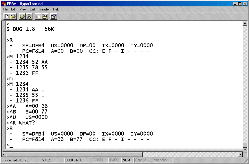
Some of the KBug9 commands are:
I [S/K] Enable Input device (Serial/Keyboard)
O [S/V/P] Enable Output device (Serial/VDU/Printer)
P [start]-[end] Punch S1 Tape
L Load S1 Tape
E [start]-[end] Dump Memory
M [addr] Memory Examine & change
R Dump registers
G [addr] Execute Program
S display S stack pointer & Dump registers on stack
^A AccA examine & change
^B AccB examine and Change
^C Condition Codes
^U Ustack pointer
^X X Index register
^Y Y index register
^P Program counter
20th Aug 2005
Bug Fix on LSR8
There is an error in the LSR8 instruction in CPU09. LSR8 was treated in the same way as LSR16, which was OK on the dual operand instructions as the high byte of ACCA and ACCB was set to zero on the left input to the ALU. For single operand instructions however, the data byte is read into the low byte of the MD (Memory Data) register and bit 7 is sign extended to the high byte. This was to support signed offsets in the branch instructions. This meant that the LSR8 instruction would operate like an ASR8 instruction with the sign bit being preserved. The fix was to place the ALU_LSR8 ALU operator with the ALU_ROR8 and ALU_ASR8 operators. This bug was spotted by an astute opencores user.
17 Sep 2005
Bug Fix on JSR, EXG CC and TFR CC
Two more bugs were brought to my attention.
The first was that EXG and TFR instructions did not work on the condition code register. Extra cases had to be assigned to the ALU to set the Condition Code output register to the Left ALU input for the ALU TFR operation.
The second problem was to do with JSR [0,S]. The indexed jump to subroutine pre-decremented the stack pointer ready to push the return address before the indexed addressing mode was calculated. This had the effect that JSR instructions indexed to the stack would get the wrong vector address. The solution was to defer the S Stack pointer decrement until after the indexed addressing mode microcode and add an extra cycle to the JSR microcode state. this required minimal effort. Note also that the JSR extended instruction gained an extra cycle as it shared the JSR microcode state.
12th Jun 2006Fixed Bug in ASR, LSR, ROR
Fixed bug in CLR
After some exhaustive testing of the single operand instructions, comparing an EF68A09 system to System09 on a Spartan 3E starter board, I found some errors in the ASR, LSR, ROR and CLR handling of the Overflow (V) Flag. ASR, LSR and ROR modify the V bit on the 6800, but not the 6809, so I had to disable the code in the ALU of CPU09 that modified the VFlag. Also the CLR instruction did not reset the V Flag. This is now fixed too.
7th July 2006
Fixed bugs in NMI.
CPU09 Version 1.13
Disable NMI on reset until S Stack pointer has been loaded. Added nmi_enable signal in sp_reg process and nmi_handler process.
11th July 2006
Fixed bugs in MUL, RTI, SYNC, DAA and Interrupt Processing of CPU09.
CPU09.vhd Version 1.14 - 11th July 2006
1. Added new state to RTI called rti_entire_state. This state tests the CC register after it has been loaded from the stack. Previously the current CC was tested which was incorrect. The Entire Flag should be set before the interrupt stacks the CC.
2. On bogus Interrupts, int_cc_state went to rti_state, which was an enumerated state, but not implemented anywhere. rti_state has been changed to rti_cc_state so that bogus interrupt will perform an RTI after entering that state.
3. Sync should generate an interrupt if the interrupt masks are cleared. If the interrupt masks are set, then an interrupt will cause the the PC to advance to the next instruction. Note that I don't wait for an interrupt to be asserted for three clock cycles.
4. Added new ALU control state "alu_mul". "alu_mul" is used in the Multiply instruction replacing "alu_add16". This is similar to "alu_add16" except it sets the Carry bit to B7 of the result in ACCB, sets the Zero bit if the 16 bit result is zero, but does not affect The Half carry (H), Negative (N) or Overflow (V) flags. The logic was re-arranged so that it adds the MD register or zero so that the Carry condition code is set on zero multiplicands.
5. DAA (Decimal Adjust Accumulator) should set the Negative (N) and Zero Flags. It will also affect the Overflow (V) flag although the operation is undefined in the M6809 Programming Reference Manual. It's anyone's guess what DAA does to V although I found Exclusive ORing Bit 7 of the original ACCA value with B7 of the Decimal Adjusted value and Exclusive ORing that with the pre Decimal Adjust Carry input resulting in something approximating what you find on an EF68A09P.
25 Feb 2007
New Directory Structure
In an attempt to rationalize the directory structure, I've created the following structure in the zip file:
System09
docThe idea is that a new directory can be created for each new FPGA board implementations and vendor specific components such as block RAM can go in a separate folder. Currently I have folders for 4K Bit Spartan 2 block RAM/ROMs and for 16K Bit Spartan3/3E Block RAM/ROMs.
rtlSpartan2 (RAM & ROMS)src
Spartan3 (RAMS & ROMS)
System09_BurchED_B3 (project files)
System09_BurchED_B5-X300 (project files)
System09_Digilent_3S200 (project files)
System09_Digilent_3S500E (project files)
System09_Xess_XSA-3S1000 (project files)
Testbench
VHDL (Common IP Cores)Flex9tools
KBug9
KBug9s
Noice
Sbug
Sys09bug
Tracebugas09
epedit
romdiskI have attempted to use generics to define operating clock frequencies and timing parameters in the keyboard and VDU. This is only a snap shot release and is still a work in progress. Only the B5-X300 and XSA-3S1000 versions have been synthesized so far, and even those are not guaranteed to work properly.
The project files have been implemented using Xilinx Webpack 7.1. The advantage of this is that they are small and they are upwards compatible with later versions of Webpack. Project files for Webpack 8.1 and onwards get very large and
2nd July 2007
Various Changes
Updated Sys09Bug to include RAM disk drivers. I have also added an XModem compatible downloaded for the RAM Disk. It appears to download a RAM disk image of Flex9 correctly using hyperterm although there appear to be problems with the disk image I am using. Sys09bug partially implements some of the features found in the MicroBox2000 found on the Flex User Group FTP Site. It includes vectorable disk drivers for each drive so it is possible to have 2 RAM disk drives as well as a Flexnet drive on a PC.
On the B5-X300 version, Flex must be loaded into memory manually due to the limited Block RAM in the Spartan 2. The B5-X300 version has a Compact Flash interface, and Sys09bug includes a CF disk boot although the CF drivers have not been implemented for Flex yet and I have yet to create a disk image for the CF with the appropriate bootstrap loader. It should be possible to used the extended memory as a RAM disk, although that feature has not been implemented yet.
On the Spartan 3 starter board Flex is stored in RAMB16 which is mapped into memory. It does not have a CF interface, although it may be possible to store a boot disk image in the configuration flash. It is designed to use the extended RAM as two RAM disks.
The XESS XSA-3S1000 I have added a timer, bus trap logic and IDE interface. I have managed to add 8 Kbytes of RAMB16 to run Flex. This was achieved by sacrificing the RAMB16 used for the colour attribute memory in the VDU and using distributed memory for the key map table in the PS/2 keyboard. There were already 2 x RAMB16 blocks left over in the previous version. All 24 RAMB16 block have now been used. As of 2nd July 2007 1:52am the design had not been tested. The SDRAM interface has yet to be implemented. Without cache, the SDRAM is very slow taking up to 8 clock cycles at 50 MHz to perform a read or write so it will slow the CPU down by a factor of 4.
The Spartan 3E starter board design has not been updated yet.
A big thank you to David Burnette who has sent me an updated version of the UART Baud clock generator that scales the size of the divider counter to match the baud rate. This has been implemented on most of the board support packages.
15th July 2007
Flex running on CF Card
No real changes in hardware, but a few software utilities have been added to support formatting and downloading Compact Flash disk images. A CF version of Flex9 is now running on the B5-X300 board.
25th January 2008
XESS XSA-3S1000 now works with SDRAM
The XSA-3S1000 port of system09 now works with SDRAM. System09 only uses 1Mbyte of the available 32 MBytes. It uses the XESS SDRAM controller running at 50 MHz. The CPU runs at 25 MHZ, but must use 4 clock cycles for a read and 3 clock cycles for a write. Further work needs to be done to implement a cache controller. Only the bottom 8 bits of the SDRAM are used as there is no byte control on the XESS SDRAM controller.
A Compact Flash interface has also been included. I need to clean up the FLEX implementation so that there is a standard Compact Flash version and clean interface to download disk images. There is a ROMed version of FLEX9 in this design, but it does not work with the CF card interface.
I also need to look at producing some documentation for the design.
5th February 2008
XESS XSA-3S1000 Boots Flex9
This is snapshot is mainly a software update for Sys09bug and Flex9.
There are 3 flavours of Flex9
Flex9_cf8 - Flex for Compact Flash mapped at $E040 with 8 bit transfers (Used on B5-X300)
Flex9_ram - Flex with RAM disk drivers (Untested) (Used on Spartan 3 Starter board)
Flex9_ide - Flex for and IDE drive mapped at $E100 with 16 bit transfers (Used on XSA-3S1000/XST-3.0)
There are 6 flavours for Sys09bug
Sys09ads - For Ackerman Digital 6809 S100 board
Sys09swt - For SWTPc compatible computers
Sys09xes - For XSA-3S100/XST-3.0 with 16 Bit IDE interface
Sys09s3s - For Spartan 3 starter board with RAM disk
Sys09s3e - For Spartan 3E starter board
Sys09b5x - For B5-X300 with CF card with 8 bit interface
For the XSA-3S1000/XST-3.0 use the UX command to download a disk image and Hyperterm with XModem protocol. Use the UF to format an empty drive. CF card should be at least 32MBytes for single drive systems or 128Mbyte for all 4 drives.
FLEXESS.dsk is the disk image for the XESS board. It takes about 11 minutes to download at 57.6KBaud.
Flex9 is included in a block RAM image on the XESS board. Once the disk image is downloaded start FLEX by setting the program counter to $CD00 using "(CTRL)P CD00" then start Flex with the "G" command.
If things are working correctly Flex should request the date then give the "+++" prompt. The files on drive 0 can be listed by the "DIR 0" command. The UX download program writes a bootstrap loader on the disk after the disk image is downloaded. The Flex image must be linked to to the boot strap using the "LINK 0.FLEX9IDE.SYS" command
25th February 2008
CPU09 CWAI & SYNC corrections
Dr Edward Cheung has been attempting to get CPU09 working on his Williams Pinball Controller. He has been having problems with the operation of interrupts, in particular FIRQ.
http://www.edcheung.com/album/album07/Pinball/wpc_sound.htm
I thought the problem might have been to do with either the SYNC or CWAI instruction.
The SYNC instruction is used to synchronize a software loop to a masked interrupt. The processor halts execution until an interrupt occurs. If the interrupt is masked, then the CPU continues on with the following instruction from the SYNC instruction. If the interrupt is not masked then a normal interrupt sequence is performed, the registers are stacked and the CPU vectors to the interrupt service routine. The 6809 manual indicated that if the interrupt is shorter than 3 clock cycles, then the SYNC instruction behaves as if the interrupt is masked. I have not implemented this feature.
The CWAI #CC instruction pre-empts an interrupt by unmasking the appropriate interrupt masks, stacking all the registers then waiting for an interrupt. This reduces the latency for processing an interrupt. The Entire flag is always set in the CWAI instruction so the return from an FIRQ must pop all the registers.
I thought we had fixed the problem, but apparently not.
The problem can be fixed by ensuring that the Entire (E) flag is always set in the interrupt sequence even for FIRQs. I'm not sure why this should be that case.
Another change I have made to CPU09 is to remove all the default register control settings from each instruction cycle so that they now reside at the start of the state sequencer process. The default register settings maintain the previous state of the register, and the default bus state is an idle on non VMA address bus state. By default the condition codes are output on the data bus.
8th September 2008
Snapshot
I renamed some of the signals and constants and added a CF interface to the BurchED B3-Spartan2+ design along the lines of the XESS IDE implementation and updated the monitor ROM for the B3 board. I also implemented a 32 x 32 hardware mutiplier register, and started work on a version for the Digilent Spartan 3 starter board using the XC3S1000.
25th September 2008
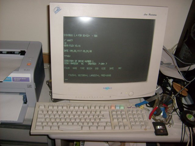
B3-Spartan2+ Implementation Runs Flex9
I have managed to get Flex9 running on the B3-Spartan2+ board with VDU PS/2 keyboard, ACIA and a variety of other peripherals. I have wired up an IDE Compact Flash adapter board using a 40 pin IDE connector and two 20 pin IDC connectors. A picture of the system is on the main FPGA web page.
The limitation of the XC2S200 is that it only has 14 x 4KBit Block RAMs rather than the 16 available on the XC2S300E. The SYSY09BUG monitor program uses 4 Block RAMs, The VDU uses 4 Block RAMs for the character generator and another 4 Block RAMs for the text buffer. One Block RAM is used for the PS/2 keyboard key map look up table, and the remaining Block RAM is used as a dual port interface to allow the B3-Spartan2+ board to be connected to the B5-X300. There is not enough Block RAM for a colour attribute page on the VDU. The design uses 86% of the XC2S200, so it maybe possible to implement the Keyboard key map lookup table in distributed RAM rather than Block RAM.
The IDE CF interface on the B3 board follows a similar interface to the XESS XSA-3S1000/XST-3.0. It uses a 16 bit interface mapped at $E100. Ultimately I would like all the FPGA boards to follow the same format so I can use the same version of Flex9 across all boards. The advantage of implementing a 16 bit IDE interface is that it can also be used with an IDE hard disk as well as a Compact Flash card. The 16 bit interface means that in future I may be able to implement a FAT16 file reader to read Windows formatted CF cards.
The Spartan3 and Spartan3E boards currently do not have a IDE or Compact Flash interfaces although an IDE CF interface has been made by someone else for the Spartan3 Starter board rewiring a Digilent 40 pin Test Point Header board.
The following is a picture of Flex9 running on System09 on the B3-Spartan2+ board. It displays the boot sequence and the directory of an empty drive partition on the CF card. Note that the display is white on black, although the photo appears to have a slight green tinge to it. I think that has more to do with the camera than anything else.
3rd December 2008
Hardware Flow Control / Makefile changes (Work in progress)
I have attempted to include hardware flow control in the monitor ROM. This is an attempt to get the B3-Spartan2+ and B3-X300 working with the Lantronix Xport card. The Lantronix Xport allows the FPGA Flex system to be accessed over the internet using a hyperterm terminal session. For some reason Hyperterm Xmodem up loads to the Flex system did not work over the internet. I don't know if this is due to flakey software in the Xport card, or if there are over run errors in the ACIA. I have elected to implement hardware flow control such that RTS is only asserted when the Flex system polls the ACIA and data is not transmitted unless the Xport asserts CTS to the FPGA system. This is a software modification that has only been implemented in some of the monitor ROMs.
As at the 3rd of December these changes have not been carried over to the RTL implementation and have not been tested.
David Burnett implemented a Makefile that allows you to to build versions of the monitor automatically. It assembles the Sys09bug monitor or Flex program and builds a ROM out of a series of 16Kbit Block RAMs. The Makefile uses S19toVHD.cpp which was only designed to initialise the Spartan 3 16KBit Block RAMs. The program previously initialised separate 16KBit Block RAM components then glued them together to produce a 4Kbyte monitor ROM or 8Kbyte Flex ROM.
I have modified this code to generate 4KBit Block RAMs found in the the Spartan 2. The actual procedure that generates the ROM, "glues together" a series of 4Kbit Block RAM components to generate the one ROM. The glue logic for the 4K Bit Block RAM scales according to the size of the ROM requested. I would like to carry this approach over to the 16KBit block RAM initialiser so that the enitire ROM is generated in the one pass.
This is a work in progress. The ROM changes have not yet been carried over into the RTL design and have not been tested. I'm uploading the files on the web page for safe keeping.
23rd February 2009
ACIA Update / S19toVHD.cpp Update
Hans Hübner has given me a ACIA update. He tells me that the ACIA had a problem with double buffering the the transmit data so had problems transmitter data at the full data rate.
Also Prof Marco Winzker from Hochschule Bonn-Rhein-Sieg, University of Applied Sciences has recommended merging the vga_clk with the cpu_clk on system09_digilent_3S200 and placing a timing constraint on the cpu_clk in the user constraint file.
I have not had time to check the cpu_clk and vga_clk on the Diligent_3S1000 or the Xess_xsa3s1000 versions.
A big thanks to Marco and Hans for their help.
I have also had another hack at the S19toVHD.cpp conversion program for generating Block RAM images, The ROM generator for the BRAM16_S9 Block RAMs now scales up according to the size of the address range specified. I also had to build in a special case when there is only one Block RAM used in the wrapper. It appears to work, but could do with more testing.
Sys09s3s.vhd is the 4KByte mon_rom wrapper
Sys09s3s_b4.vhd is a 2K ROM module using 4 x 4Kbit block RAMs found in the Spartan 2
Sys09s3s_b16.vhd is one or more 2K ROM module using 1 x 16Kbit block RAMs found in the Spartan 3
The makefile generates both a _b4.vhd and _b16.vhd file for the motorola S19 file.
Note that for the Spartan 2 boards there is not enough Block RAM for a 4KByte monitor so I only use the _b4.vhd module. There needs to be a more general way of building ROMs.
I've tested the Digilent 3S200 and the XSA3S1000 boards with the new ROMs but I have not had time to test the other implementations. I did not get around to updating the ROMs on the Digilent 3S500E board implementation.
25th February 2009
SPI Master added
Hans Hübner kindly has added an SPI Master controller to the project. It's in the System09/rtl/VHDL/spi-master.vhd
Back to FPGA Page