The first step was to create a top level graph that represented the processing data flow. The graph consisted of function boxes and interfaces that were programmed to accept input and produce output with the estimates delay provided by the HDI and MSE designers. The initial graph was designed to reflect the system data flow, with all functional boxes on the graph stubbed out. When the prototype hardware became available, the top level graph was executed on the Alex processing boards. Using this top level HighClass DFG we were able to evaluate the data communication and quering design and refine the strategy for distributing the MSE LRC, MSE HRC and MDI processing functions. The analysis of the top level graph timing results uncovered that partitioned, mapped and static data flow would not achieve the required processor utilization. As a result, changes were made to the top level graph to include queues, multiplexers and dynamic data flow. This top level graph is shown in Figure 1. Emulation results showed that communications had to be overlapped with processing to meet the timing requirements. Evaluation of timing results also identified changes needed to GEDAE™ to allow the user to specify the size of the communications buffers. In addition, changes in the GEDAE™ scheduling algorithm were needed to enable more efficient multiplexer operation. Finally, the processing timeline generated by this flow, shown in Figure 2, verified the intra-board communication bandwidths were high enough for the HighClass application.
The second goal of the top level graph was to verify control processor/DSP board communications. A simple control program interface was integrated with the top level graph to test VME communications speeds. This integration served to solidify the functional interface from the host to board, in terms of data types and sizes being transferred. Tests of the graph using the control program revealed that host to board communication speeds were slower than expected. These results led to changes in the GEDAE Alex port to improve DMA data transfer between the host and DSP boards. The tests also exposed the need for large memory buffers to support efficient overlapped communications and processing for the large data sets. The need for these large buffers further revealed memory limitations in the operating system software, which were fixed by Alex. The resulting host to board communications rate was measured as 8 Mbytes/sec which was approximately three times greater than the rate needed to meet the BM4 requirements.
As the final MSE and HDI DFGs were integrated with the top level graph, changes were made in the system level data flow. These changes were not incorporated in the original top level graph. As the top level graph became more complicated, graph partitioning and timing optimization efforts became cumbersome. In retrospect, many of the problems encountered during these final system integration and test efforts could have been more efficiently resolved by maintaining a simple timing version of the top level DFG, and using it to optimize data flow between the HDI and MSE DFGs.
In summary, a top level graph was developed and executed on the target processing board to verify the host to board and intra-board communications rates. The top level graph development activity identified a number of areas where improvements were needed to achieve the required processor utilization. The top level graph was developed several months prior to final integration, providing sufficient time to correct the problems without impacting the final system integration. As a result, many of the issues associated with processor utilization, memory utilization and communication rates were resolved before final integration. Finally, the top level graph would have been even more useful if it had been maintained and used to test and verify the data flow refinements during the HDI and MSE classifier DFG integration.
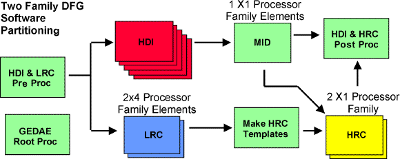
A graphic depicting the functionality of the DFG developed to process 10 images per second is shown in Figure 3. The graph was designed using GEDAE™s family syntax which provides the facility to distribute multiple instances of a function across multiple platforms. The initial DFG used two MSE-LRC families, each consisting of four processors. It used a family of 16 HDI processor, as well as 3 MSE-HRC family elements. The purpose for the individual functions in this figure are described in Table 1. Sixteen images could be simultaneously processed in HDI, while two images were simultaneously processed in each stage of the classifier. Queues were placed in this graph to offset the variations in the processing rates of HDI and the MSE classifier functions.
|
Function |
Purpose |
Number of Simultaneous Instances |
|
HDI & LRC Preprocessing |
|
1 |
|
HDI |
|
16 |
|
Mid |
|
1 |
|
LRC |
|
2 |
|
Make Templates |
|
1 |
|
HRC |
|
2 |
|
Post Processing |
|
1 |
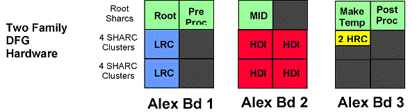
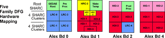
GEDAE was used to generate the code to execute this DFG on the Alex processing boards. The mapping of the software functions onto three Sharc boards is shown in Figure 4. The two families of the first MSE-LRC classifier were mapped to eight Sharcs on the first Alex board, the HDI functions were mapped to 16 Sharcs on the second board, and the two families of the MSE-HRC classifier were mapped to two SHARCs on the third board. The preprocessing, mid, make templates and post processing functions were all mapped to root SHARCs on the three boards since these functions needed external memory.
Several problems were discovered when this graph was executed on the embedded processors. The processors performing the HDI functions had to transfer intermediate results to the mid processor before they could continue. The initial execution timelines for this graph indicated the HDI processors were performing much slower than expected, because the 16 processors were simultaneously communicating intermediate results to the mid processor. The HDI output queue sizes were increased and were placed in the SRAM external memory of the mid processor. After these changes, the HDI processors were able to process an image in 1.7 seconds versus the 1.42 seconds in the standalone HDI DFG. The other problem identified with the smaller graph was that the preprocessor was not processing images fast enough to keep the HDI and LRC processors busy. Upon examination, it was found that the GEDAE Alex port queue management was not being performed efficiently. Changes were made to this port which eliminated the problem.
Since each HDI processor needed 1.7 seconds on average to process an image, it was readily apparent that the 72 SHARC processors could not meet the 30 images per second goal. Since each LRC family was able to process 5 images per second, the final DFG implementation was designed to process 25 images per second. A graphic depicting the final GEDAE DFG is shown in Figure 5. This graph contained five families of LRC, three families for HRC, and 3 HDI families, each executing 14 instances of the algorithm.
The development of this final GEDAE™ flowgraph uncovered several new problems due to its size. First information about GEDAE™ functional mapping, execution schedule, memory allocation and queues is maintained in its groups settings file. These settings are typically set using the GEDAE GUI. However, the file for this graph was so large that the data could not be displayed within the X windows display. As a result, the group settings file had to be manipulated outside of GEDAE™ tool using a text editor. Excel was selected as the preferred editor to manipulate the data in the 28,000 line group settings file because of its column editing capabilities.
The GEDAE™ tool determines the schedule for each of the individual embedded processors. Queue placement, firing granularities and execution priorities are controlled by GEDAE™ to reduce the schedule complexity. The biggest challenge in generating the final graph was the placement of queues in the appropriate locations to reduce schedule complexity. The full GEDAE top level flow graph is shown in Figure 7 and shows the placement of the final queues. The initial execution schedules were too large to view within GEDAE™. As a result, we had no insight to determine how the queues, firing granularities and priorities could be adjusted to simplify the schedule. Changes were needed in GEDAE to display the schedule in a collapsed format to provide the visibility we needed to refine the schedule.
Difficulties were also encountered in executing the initial full DFG. Schedules for all of the processors were being generated correctly and down loaded to each of the processors. However, the graph would not execute. This problem was very difficult to isolate. The problem was finally identified by scaling back the size of the full graph. The problem was the preprocessor was trying to open 180 data ports to pass the input images to the 62 processors performing HDI and LRC functions. GEDAE™ was not able to open up this many ports. This problem was circumvented by reducing the number of ports to 100 by combining the data ports to the HDI processors. This problem would have been found earlier in the design process if the top level graph, described in the previous section, has been maintained to verify data flow changes in the final DFG.
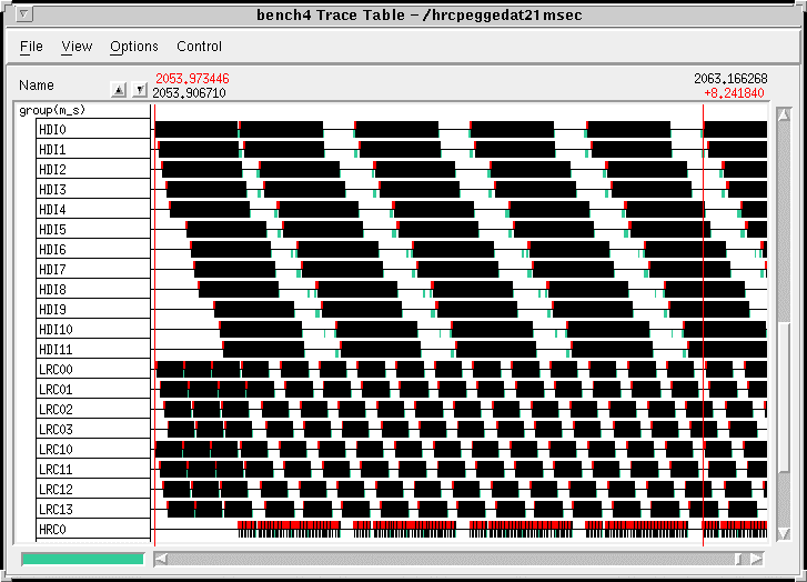
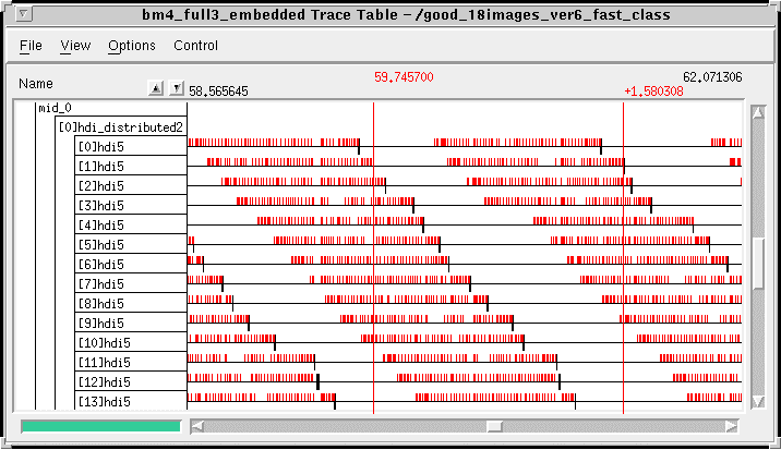
While the integration of the final DFG was cumbersome due to its large size, we were able to develop the flow graph, isolate and resolve the problems, and optimize it in less than two weeks. The performance achieved on the 72 processors was impressive. All of the SAIP functional requirements were met with the only differences in the classification scores, due to the Sharc single precision implementation. As expected, the image chip throughput performance of this graph was limited by the five first stage classifiers. This graph processed images at a 25.4 images per second rate as shown in Figure 8. To determine the maximum processing rate for the 42 HDI processors, parameters for the classifier were adjusted so the overall graph performance would be limited by the HDI subsystem. This graph processed images at a 26.5 images per second. The trace table depicting the processing timeline for one of the mid processors collecting the intermediate results from 14 HDI processors is shown in Figure 9. The requirement for each HDI processor to send its intermediate results to the mid processor before processing the next subregion reduced the single image HDI DFG performance by approximately 13 percent. The aggregate processing efficiency (intrinsic rate/peak processing rate) of the 65 processors performing the HDI and MSE classification algorithms was 21 percent. This efficiency dropped to 19 percent when averaged over all 72 processors. The final flow graph achieved a 92 percent processor utilization rate (time that a processor is actively processing) for the 65 processors performing HDI and MSE.
The two primary lessons learned in the development of the final DFG were:

The control program was developed by adapting the original SAIP C++ control code. Minimal changes were made to the original code and data class structures, used to pass messages among the SAIP host system processes, were preserved.
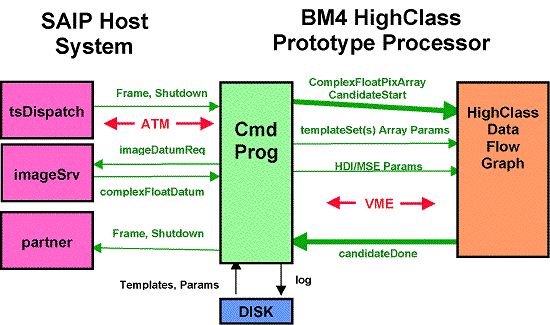
The control program communicated with the SAIP system using of SAIP defined message types passed through an ATM physical interface. The control program exchanged data with the HDI and MSE DFGs through GEDAE's command language interface. This interface was used to pass control parameters to the DFGs during initialization, control the switching between modes, place images on the input queue and take HDI and MSE results off output queue. Data was passed between the control program and DFGs using the VME backplane. The Application Interface Builder (AIB) the tools were used to automatically generate all of the command program software for controlling the GEDAE™ DFGs.
Once the control program was developed, it was integrated and tested with the SAIP system emulator and an early version of the top level DFG. Functional testing was initially performed with the DFG executing on the Sun workstation. After the functional performance was verified, the control program was integrated with the early version of the DFG executing on the Alex boards. Initial testing uncovered problems with the VME backplane speed. The problem was isolated to a DMA memory addressing issue on the Alex boards. Once this problem was corrected, the control program was able to keep the embedded processors loaded at over 30 images per second.
After the final DFG had been tested, it was integrated with the HighClass control program. No significant problems were encountered as the operation of the control program had been verified with an earlier version of the DFG.
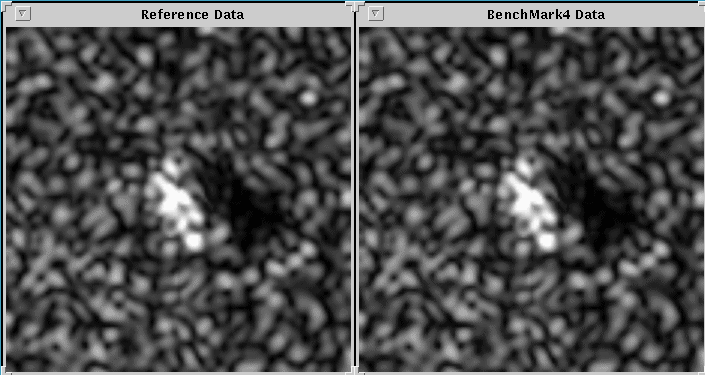
The performance of the integrated HighClass prototype was characterized during the final acceptance test. The BM4 processor passed all functional tests. The images generated by the embedded HDI algorithm were judged to be visually equivalent to images generated by the executable requirement. Output images from the BM4 processor and executable requirement for a T72 tank input SAR image are shown in Figure 11. The MSE classifier also met functional requirements with a normalized classification score error of 0.0055 versus a 0.006 requirement. The identical five target classes were output by the embedded classifier for all test image chips. In addition, the rank order for the five output target classes was identical for both the BM4 processor and the executable requirement for the 70 test cases with the exception of adjacent target classes switching rank order position 6 times (out of a total of 350 positions). The BM4 processor passed the extensive set of tests used to verify that all frame processing requirements were met. The acceptance test demonstrated that the BM4 processor could continuously process images at a 22 images per second rate. This rate was slightly less than the 25.4 images per second rate achieved with the DFGs operating without the control program. Analysis of the acceptance test results indicated that this slow down was caused by delays interjected by the operating system on the control board. These delays could have been avoided if a real time operating system had been used on the control board.