Approach
Unlike the FPGA custom board virtual prototyping activity token-based lightweight VHDL performance models were used to model the C80 and C6201 board architectures. The VHDL models used for developing the C80 and C6201 models, made extensive use of existing DSP and network communication models from the RASSP reuse library.
Based on a preliminary design of the C80 MSE software, it was estimated that the low resolution processing would take an average of 3.2 clock cycles per pixel to execute the low resolution MSE target match. For high resolution matches, where the raster vector lengths are significantly longer, it was estimated that 2.12 clock cycles per pixel would be required. TI supports two versions of the C80 DSP that run at 40 MHz (25 nanoseconds instruction time) or 60MHz MHz (17 nanoseconds instruction time). Using these timing rates, the number of instruction cycles and the total number of pixels processed per pose angle, functional timing estimates were establish for the C80 CPUs for performing the low and high resolution MSE template matches. Similarly, timing estimates for the C6201 were established. The C6201 DSP runs on a 200 MHz clock or 5 nanoseconds per instruction cycle. In the case of the C6201 it was estimated that the low resolution processing would require an average of 3.5 cycles per pixel and the high resolution processing was estimated to require 1.85 cycles per pixel. The estimated C80 and C6201 Processing and timing estimates are also summarized in table 2.
Data transfers between the C80 external I/O interface and the internal CPU data RAM use 32 bit wide data paths and operate at the chip clock rate. As a result, the internal C80 bus was modeled as a 160 MB/second data bus for the 40 MHz C80 and 240 MB/second for 60 MHz version. The board control/data bus was designed and modeled as a 64-bit wide bus, running at one half the 40 MHz or 60 MHz C80 clock speed, reflecting the C80�s 64-bit wide input data interface. The template memory was designed to use 64 bit wide data words using 50 or 40 nanosecond DRAM to match the C80 160 or 240 MB/second data rates.
In the C80 architecture each of the CPUs has 6 Kbyte of data RAM, split into three 2 Kbyte data banks. To map the MSE function onto the C80 DSP architecture, consideration had to be given to the amount of image chip and template data that could be stored in each CPU's RAM. To reduce contention on the C80 internal crossbar, the most efficient design was to have each CPU operate on data within its own data RAM. This limited the maximum number of pose angle templates that could be loaded at a one time and required that the templates be read in sequentially as each image chip was processed.
The size of the low resolution image chip was less than 2 Kbytes and was stored in one of the 2K banks of the CPU DRAM. The remaining 4 KB of RAM was used to store template data. The average, low resolution template size was about 400 bytes. As a result, only nine templates at a time could be read in and processed. In order to process a single target class, with 72 pose angles, 8 template sets had to be processed sequentially.
MSE low resolution data flow processing was initiated by the board control processor sending a low resolution image chip to each of the C80s. Each of the four on chip CPUs received the same image chip. Once the CPUs received the image chip data, the first 9 templates were read in and the individual template matches were performed. This process was repeated 8 times for each of the five target classes. The other fifteen target classes were simultaneously processed by the other three C80 CPUs. When the low resolution processing was completed, the CPU notified the C80 RISC processor and transferred the pose angle, dither location and best MSE score for each of its� 5 classes.
When all four CPUs completed the low resolution processing, the RISC processor notified the board controller and transferred the data for all 20 target classes. The same process was performed by each of the four C80s. When all four C80s notified the control processor that they had completed low resolution processing, the control processor sent the high resolution image chip data to all 4 C80s. This synchronized the initiation of the C80s high resolution processing. There was a slight loss of compute time for the CPUs that completed the low resolution processing early. However, simulation results showed that with the static assignment of classes, the variance in low resolution processing times was less than 10%.
Since the high resolution image chip spans two CPUs, there was the potential for contention between the CPUs when accessing the image chip data. When contention occurs, the C80 uses round-robin arbitration to allow one CPU to access the RAM during the first cycle and then the other CPU is given access during the next cycle. Thus, one CPU must wait an extra clock cycle to receive its data. To reduce the probability of contention, each CPU pair processed the same pose angle template. They initiated processing at opposing dither locations. With 49 dither locations per pose angle template, the first CPU processed 25 dither locations starting at the top of the image chip while the second CPU processed the remaining dither locations starting from the bottom. Although they each process the full template at each dither location, the number of pixels requiring access to the others RAM was significantly reduced.
A second reason for having the two CPUs process the same pose angle was to balance the distribution of the processing. There were 14 pose angle templates to be processed for each class in high resolution mode. The 14 pose angle templates for the 5 target classes did not divide evenly across four CPUs. On the other hand, having two CPUs process the same pose angle template allowed the 14 pose angle templates to be evenly distributed between the two CPU pairs.
After all the C80's completed the low resolution processing, the board control processor initiated the high resolution processing by sending the high resolution image chips to the individual CPUs. The first 4000 bytes of the image chip were sent to the first CPU and the second half was downloaded to the second. The same data was also sent to the second CPU pair on the C80. Different high resolution image chips were sent in the same manner to the other C80s on the board.
When each CPU received its high resolution image chip data, it fetched the first pose angle template for the first of its five classes. CPUs 1 and 2 fetched the same pose angle template, formatted in opposite order. CPUs 3 and 4 fetched a different template formatted in the same manner. Each CPU processed the entire template for half the dither locations. When a CPU pair finished processing a template the next template was fetched and processed. The 14 pose angle templates were split between the two CPU pairs. The odd numbered poses, were assigned to CPUs 1 and 2, and the even numbered ones were assigned to CPUs 3 and 4. When the CPUs finished processing the templates for the first class, they continued fetching and processing the templates for the next class until all five target classes had been processed. When all five classes were completed, the RISC processor was notified and the MSE processing results were transferred. When the RISC processor received notification from all the CPUs, it notified the control processor and transferred the final MSE scores and best positions for each of the five classes.
When the control processor was notified by all four C80's that they had completed high resolution processing, the control processor repeated the cycle by sending the next set of four low resolution image chip data to the C80's.
Separate statistical models were used in low resolution and high resolution processing models. The models consisted of the minimum and maximum number of pixels processed as a function of class type and pose angle. A random process was used to vary number of pixels processed between the minimum and maximum for each pose angle and a variable performance time token was computed.
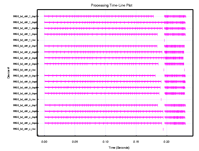
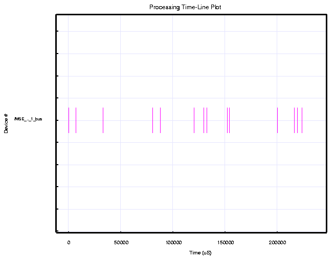
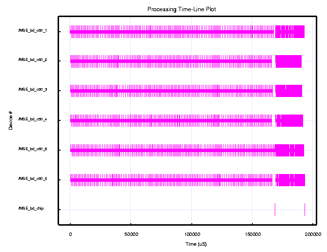
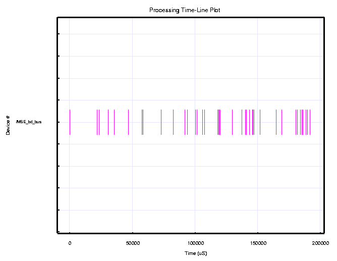
A blow-up of the timeline for the processing of the first image chip is shown in Figure 3. This figure illustrates the randomness in the completion times due to different sized templates and statistical early termination. Figures 4 and 5 show the bus utilization for the same period, for the on-chip bus model and the board level bus model, respectively. The board level bus timeline shows much higher bus utilization than the on-chip bus utilization, as expected. However, these graphical sketches actually over exaggerate the utilization due to the nature of the plotting ink.
Actual bus and processor utilization were recorded during simulation and are summarized in the following table.
The bus utilization was shown to be very low, resulting in minimal bus contention and high processor utilization. The sum of the four local bus times are slightly larger than the board-level bus time indicating that there was some waiting at the local bus for the board-level bus to clear. This time was computed to be 6.4% of the total data transfer time for each local bus.
The average processor utilization across all 16 DSPs is 94.383%, which was quite highly efficient. This is due to the highly repetitive nature of the MSE algorithm and relatively low bus activity.
In summary, the results of the C80 (40 MHz) virtual prototype verified that two VME 6U boards having four DSPs could process 34 image chips per second and meet the MSE requirement for processing 30 image chips per second with a 13% margin. Partitioning of the MSE processing tasks was shown to be straightforward by assigning of each C80 to a single image chip for both low and high resolution classification processing. The control software used a straight forward design and a simple on-board bus architecture with a single low and high resolution template memory was shown to be sufficient. Furthermore, a software design strategy was developed and verified for partitioning the image chip, template data and processing tasks to fit in the 8 Kbytes of C80 on-chip memory.
Finally, while the current simulations used static class assignments and synchronized the start of low resolution processing and high resolution processing for all C80's, the software design could be made dynamic to increase the image chip throughput. In the future, if early termination computation times result in greater variances, a dynamic scheduler could be added to the C80 RISC processor to more evenly distribute the processing. In addition should addition processing efficiently be required the MSE processing on eachC80 could be started independently and not have to wait until the other DSPs have completed processing. Using these two enhancements, the overall throughput performance could be improved.
C80 (60 MHz) Custom Board Simulation Results
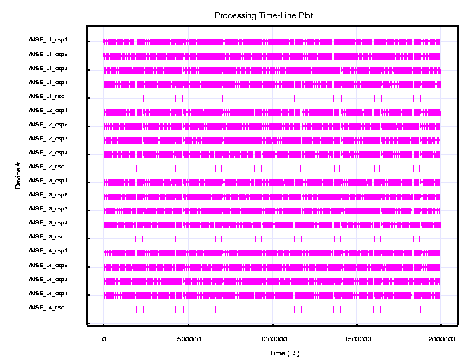
Figure 6 shows a timeline for the C80 (60 MHz) for a two second simulation. The timelines show all 16 DSPs first doing the low resolution computations for a period of about 132 milliseconds, followed by the high resolution computations for approximately 28 milliseconds. They all repeat this process continuously. During the two second simulation interval, each c80 processes 12.5 image chips, resulting on a total of 50 image chips being processed by all four c80's. Based on these simulation results, we established that a C80 (60 MHz) custom board could support a sustained 25 image chips per second throughput rate.
Again an expanded view of the timeline for the processing of the first image chip is shown in Figure 7. The randomness in the completion times due to different sized templates and statistical early termination is more visible in this figure. The on chip and board level bus timelines again showed that bus utilization and contention were minimal. However, these graphical sketches actually over exaggerate the utilization due to the nature of the plotting ink.
Again the actual utilization for the buses and processors were recorded during simulation and are shown in the following table.
The sum of the four local bus times were again slightly larger than the board-level bus time indicating that there was some contention on the local bus for the board-level bus to clear. This time was computed to be 6.9% of the total data transfer time for each local bus.
The average processor utilization across all 16 DSPs was 94.132%, which is highly efficient, due to the repetitive nature of the algorithm and low processor communication activity.
In summary, the results of the c80 (60 MHz) virtual prototype established that two VME 6U boards having four DSPs, could process 50 image chips per second and meet the MSE requirement for processing 30 image chips per second with a 67% margin. As in the case of the 40 MHz virtual prototype, partitioning the MSE processing tasks was straight forward, a simple on-board bus and single template memory met the requirements, and the image chip, template data and processing tasks were sized to fit in the 8 Kbytes C80 on-chip memory.
In partitioning and mapping the MSE the low and high resolution processing tasks, static class assignment was used. However, if in the future, due to greater variances in early termination completion times, a dynamic scheduler could be added to the on-chip RISC processor to more evenly distribute the processing load. In addition should increased processing efficiently be required the MSE processing on each C80 could be started independently and not have to wait until the other DSPs have completed processing. Using these two enhancements, the overall throughput performance could be improved.
Each C6201 DSP has 64 Kbytes of on-chip program memory and 64 Kbytes of on-chip data memory. This provides ample memory to load the image chip and at least nine low resolution templates or one high resolution template.
When the low resolution processing was completed, the c6201 notified the control processor and transferred the best score for each of the 20 classes. When the control processor was notified that all six C6201's had completed the low resolution processing, the control processor sent the high resolution image chip data. This synchronized all DSPs to start the high resolution processing at the same time. While there is some lost time for the DSPs that completed the low resolution processing early, simulation results showed the variance in processing times was less than 5%.
In the case of the high resolution, the five best classes from the low resolution are processed, for fourteen pose angles, and at 49 dither. Each C6201 processes all five classes for its� high resolution image chip.
When a C6201 received the high resolution image chip data, it fetched the first pose angle template for the first class and performed the high resolution target match. The fourteen pose angle templates were loaded and processed in succession. This process was then repeated until all five target classes have been completed. When a C6201 finished processing all five classes, it notified the control processor and transferred the final classification scores and best pose angles for each of the five target classes.
When all six C6201s have completed high resolution processing, the control processor repeated the cycle by sending the next six low resolution image chips. This process synchronizes all C6201 DSPs to start the low resolution processing at the same time.
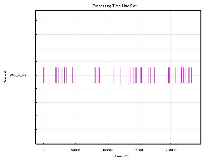
A blow-up of the timeline for the processing of the first image chip by each C6201 is shown in Figure 10. The randomness in the completion times due to different sized templates and statistical early termination is more visible in this figure. Figure 11 shows the bus utilization time for the same period, for the board level bus model.
Actual utilization for the bus and processors was recorded during simulation over the two second interval and are tabulated in the table below:
The average processor utilization across all six C6201 DSPs was 96.18%, which is again extremely efficient as a result of the repetitive nature of the algorithm and low level of bus activity.
In summary the use of performance modeling for the 200 MHz C6201-based MSE application proved quite useful in evaluating a number of C6201 custom board architectural issues. It verified that the development or purchase of a VME 6U board having six C6201's could meet the MSE requirement for processing 30 image chips per second with a 3% margin. Partitioning of the tasks was shown to be straightforward with the assignment of each image chip to a separate C6201. The MSE control software was shown to be relatively simple and the feasibility of using a simple on-board bus validated. In addition, a single on-board template memory for all six C6201's proved to be sufficient to handle the template storage and data transfer requirements. Each C6201 DSP contained sufficient on-chip memory to allow multiple templates to be loaded for processing. The actual number of templates used in the simulations was arbitrary and was not critical for the C6201 implementation. If it makes the programming any simpler, a larger number of templates could be loaded in the final implementation.
In partitioning and mapping the MSE, the low and high resolution processing tasks, static class assignment was used. However, if in the future, due to greater variances in early termination completion times, a dynamic scheduler could be added to the board control processor to more evenly distribute the processing load. In addition, should higher processing efficiently be required the MSE processing on each C6201 could be started independently and not have to wait until the other DSPs have completed processing. Using these two enhancements, the overall throughput performance could be improved.
Finally, since the C6201 virtual prototype simulation times is based on an average of 3.5 and 1.85 cycles per pixel for the low and high resolution processing respective, it was considered critical to verify the actual C6201 with timing benchmarks early in the detail design cycle. This was further reinforced by the C6201 sophisticated long instruction word architecture and the immaturity of optimizing C compiler. All three of these factors lead to the recommendation that the MSE algorithms be captured and tested on a C6201 or C6201 simulator/ emulator.
A summary of some of the key design factors and simulation results for the C80 (40 MHz), C80 (60 MHz) and C6201 (200 MHz) MSE custom board virtual prototypes are shown in the following table.
As shown the C80 (40 MHz) custom design had an average throughput rate of 17 image chips per second while the 60 MHz design could process 25 chips per second. Both designs required two VME 6U boards to meet the SAIP MSE processing requirement of 30 image chips per second. In the case of the C6201 custom board the virtual prototype established that a single VME 6U could process 31 image chips per second.
The MSE custom board virtual prototype results were based on estimates of the number of instruction cycles needed to perform the MSE low and high resolution computations. While the models were developed using conservative estimates of the communication and loop overhead, final throughput could vary based on the final DSP instruction counts. As a result, it was recommended that emphasis be placed on benchmarking the MSE low and high resolution timing early in the detailed design cycle. This early benchmark data was considered critical for the C6201 design where the performance margin was only 3%.
The virtual prototype preliminary software design used static assignment of the target templates. In addition, the initiation of both the low and high resolution template matching processes was synchronized for the individual DSPs by the control processor. In both instances, dynamic scheduling of the target templates or image chip processing could provide additional timing margins if benchmarks for the current software design fall short of the required processing rate.
Virtual prototyping of the C80 and C6201 MSE custom board design proved to be invaluable in resolving a number of critical hardware/software architectural issues. First and foremost the C80 and C6201 virtual prototypes provided the performance data for establishing the processing throughput rates of the candidate DSP custom board designs. This data was a key factor in the MSE custom board tradeoff analysis and selection. The virtual prototype also provided the mechanism for investigating, refining and establishing the custom board software design. The MSE low and high resolution control software was developed and verified and the feasibility of performing both the low and high resolution processing on a single DSP was established. Finally, these performance simulations clearly demonstrated that the bandwidth requirements for image chip and template data transfer were minimal and that neither a high speed interconnect network or dedicated template caches were necessary.
Using the RASSP Hardware/Software virtual prototyping tools and techniques, ATL was able to develop, refine and verify the designs of the three MSE DSP custom board designs in less than two months and fewer than 6 manweeks. Using the results of these virtual prototyping efforts ATL and the government Tri-Service RASSP Review team were able to easily identify the benefits and shortcomings for each of the candidate designs and make a fully informed decision on the final architecture design for the MSE processing subsystem.
Processing Requirements
A Mean Square Error (MSE) classifier algorithm determines which targets in a template library best match an incoming image chip. In the first stage classifier, the comparisons are done in low resolution. The incoming image chip is compared to 20 target classes, each having 72 pose angle templates and 121 dither offset positions. The best five low resolution matches from the first stage are used in the second stage to determine the best high resolution target match around a limited number of pose angles and dither positions. The MSE throughput requirement was to process 30 image chips per second, in both low and high resolution classifier. The detailed requirements for the low resolution and high resolution MSE functions are shown in the following table.
Low Resolution
MSE High Resolution
MSE Processing Rate (Chips/sec) 30 30 Number of Target Classes 20 5 Number of Pose Angles 72 14 Number of Dither Locations 121 49 Average Number of Valid Pixels 162 1231
Processing/Timing Estimates C80
(40 MHz) C80
(60 MHz) C6201
(200 MHz) Low Resolution MSE Processing Timing Estimates Aver # of pixels processed per pose angle (K pixels) 19.6 19.6 19.6
Number of pixels processed per target class (M pixels) 1.4 1.4 1.4
Total instruction cycles per target class (MFlops) 4.5 4.5 4.9
CPU Processing time per target class (Millisecond) 113 75 25
Chip processing time for 20 target classes (Millisecond) 565 376 494
High Resolution MSE Processing Timing Estimates Aver # of pixels processed per pose angle (K pixels) 60.3 60.3 60.3
Number of pixels processed per target class (K pixels) 844 844 844
Total instruction cycles per target class (MFlops) 1.8 1.8 1.6
CPU Processing time per target class (Millisecond) 45 30 7.8
Chip processing time for 5 target classes (Millisecond) 56 37 39
MSE Custom Board Virtual Prototype Implementation
To evaluate the performance and validate the preliminary hardware designs, performance models were developed for the C80 and C6201 MSE custom board designs. Descriptions of these modeling activities are provided in the following paragraphs.
MSE C80 Custom Board Hardware Model Implementation
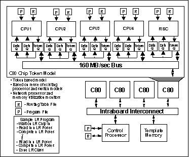
A block diagram of the C80-based MSE custom board design is shown in Figure 1. The C80 custom board design was modeled hierarchically and made up of the following components; four C80s, a control/data bus, a control processor to control the C80 DSPs and transfer the image chip data, and template memory to store the low and high resolution target templates. Each of these elements were modeled separately and then integrated into the board level performance model. The board control/data bus requirements were to be established based on the simulation results, so a simple bus architecture was used as the starting point. Each C80 DSP was modeled as four CPUs and a RISC control processor, reflecting the actual C80 DSP architecture. The interconnect on the C80 DSP is a complex cross-bar-switch. However, for the MSE custom board design, the control and data transfers were all handled via the single external I/O interface. As a result, the cross bar switch was modeled as a simple bus model with data transfers occurring between single source/destination pairs at any one time. The MSE low communication bandwidth requirements allowed the use this simplified model, which was later validated by the simulation results.
MSE C80 Custom Board Software Model Implementation
The MSE C80 software data flow was designed to have each C80 process a single image chip. With four C80's per board, four image chips could be processed simultaneously. Each C80 first performed the low resolution template matching. When all four C80's completed the low resolution processing, they were assigned a high resolution image chip. When all four completed the high resolution processing, the process was repeated for the next set of image chips.
Low Resolution Software Partitioning and Data Flow
The MSE low resolution computation requires the image chip be matched to the 20 target classes. Each class consisted of 72 pose angles and must be accomplished at 121 different dither locations. The C80 low resolution software was partitioned to have each of the four on chip CPUs process 5 of the 20 target classes. Since the templates vary in size, the 20 classes were statically assigned so each CPU was assigned 5 classes with approximately the same average number of pixels. This helped balance the computational load for the CPUs.
High Resolution Software Partitioning and Data Flow
In the case of the MSE high resolution processing, the size of the image chips and templates were significantly larger. The largest image chip was just under 8,000 bytes and would not fit in a single CPU's 6K bytes of local RAM. As a result, an approach was devised to divide the high resolution image chips and store them in the memory of two CPUs, using 4KB of RAM in each. The same image chip was also split across the other CPU pair and C80 processed a different high resolution image chip. With only 2KB of RAM left in each CPU and the largest template size being just under 2000 bytes, only one high resolution template could be loaded and processed at a time.
Software Model for MSE Early Termination Random Time Estimation
MSE functional simulations had shown that an early termination algorithm saves more than 50% of the MSE computation time. Early termination is implemented by comparing intermediate MSE cumulative scores for the current template match with the best (lowest) previous score for the target class. If the intermediate accumulative score was greater than the lowest previous score, processing of that dither location was terminated, saving the time for processing any remaining pixels. As the number of dither locations and pose angles processed for a specific target class grows, the best score decreases. As the best score decreased the number of pixels that must be accumulated to exceed the best score also drops. Statistics were captured during the algorithm functional simulations that established the variance in the number of pixels processed using early termination for both the low and high resolution MSE functions. These statistics were used to develop a software performance model that statistically varies the MSE processing times.
4.1.3 C80 Custom Board Simulation Results
4.1.3.1 C80 (40 MHz) Custom Board Simulation Results
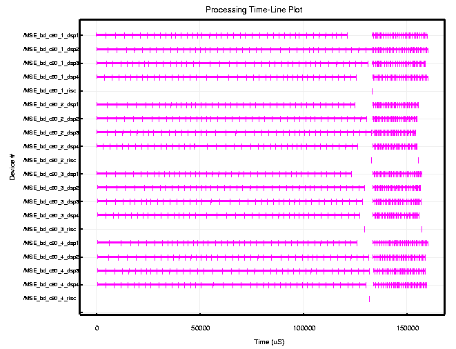
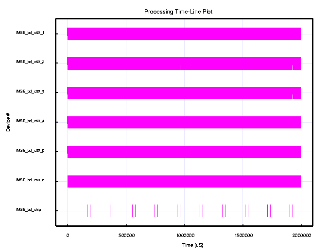
Figure 2 shows a timeline for the C80 (40MHz) custom MSE board for a two second simulation. The timeline shows the processing times for the control processor as well as C80 CPUs. The figure shows that the 16 CPUs perform the low resolution computations for a period of approximately 195 milliseconds, followed by the high resolution computation that takes approximately 40 milliseconds. Each group of four CPUs within a C80 operated on a single image chip. During the two second interval, each C80 processed 8.5 image chips, resulting in a total of 34 image chips being processed by the C80 custom board during the two second runtime. Based on these timing results, we established that the C80 custom board with 4 C80s could process approximately 17 image chips per second on a single C80 MSE custom board.
C80 (40 MHz) MSE Custom Board Simulation Results Model Component Bus Transfer Time (nsec) Bus Utilization board_bus 205,253,764 10.263%
c80_1/proc_bus: 55,246,152 2.762% c80_2/proc_bus: 54,874,229 2.744% c80_3/proc_bus: 54,978,188 2.749% c80_4/proc_bus: 54,291,814 2.715% Model Component CPU Processing Time (nsec) CPU Utilization c80_1/dsp1: 1,884,183,461 94.210% c80_1/dsp2: 1,934,899,120 96.745% c80_1/dsp3: 1,928,164,360 96.410% c80_1/dsp4: 1,895,619,476 94.780% c80_2/dsp1: 1,840,062,754 92.005% c80_2/dsp2: 1,895,482,050 94.775% c80_2/dsp3: 1,885,060,142 94.255% c80_2/dsp4: 1,835,692,811 91.875% c80_3/dsp1: 1,852,119,342 92.605% c80_3/dsp2: 1,905,595,772 95.280% c80_3/dsp3: 1,893,098,615 94.655% c80_3/dsp4: 1,853,708,347 92.685% c80_4/dsp1: 1,887,428,021 94.370% c80_4/dsp2: 1,915,043,308 95.750% c80_4/dsp3: 1,916,278,352 95.815% c80_4/dsp4: 1,880,183,937 94.010% average 94.383% 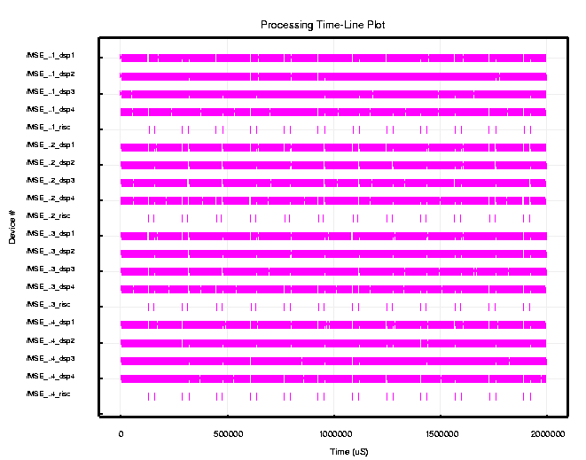
C80 (60 MHz) MSE Custom Board Simulation Results Model Component Bus Transfer Time (nsec) Bus Utilization
board_bus: 216,043,404 10.802%
c80_1/proc_bus: 58,374,177 2.919%
c80_2/proc_bus: 58,011,386 2.901%
c80_3/proc_bus: 58,226,497 2.911%
c80_4/proc_bus: 57,468,033 2.873%
Model Component CPU Processing Time (nsec) CPU Utilization
c80_1/dsp1: 1,875,474,708 93.775%
c80_1/dsp2: 1,936,482,479 96.825%
c80_1/dsp3: 1,929,793,506 96.490%
c80_1/dsp4: 1,885,472,377 94.275%
c80_2/dsp1: 1,831,737,553 91.585%
c80_2/dsp2: 1,888,720,818 94.435%
c80_2/dsp3: 1,875,378,151 93.770%
c80_2/dsp4: 1,830,150,174 91.510%
c80_3/dsp1: 1,854,860,479 92.745%
c80_3/dsp2: 1,894,035,317 94.702%
c80_3/dsp3: 1,892,293,386 94.615%
c80_3/dsp4: 1,844,827,583 92.245%
c80_4/dsp1: 1,876,314,461 93.815%
c80_4/dsp2: 1,909,863,994 95.495%
c80_4/dsp3: 1,921,419,744 96.070%
c80_4/dsp4: 1,875,255,291 93.765%
average 94.132%
MSE C6201 Custom Board Model Implementation
MSE C6201 Custom Board Hardware Model Implementation
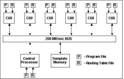
Once the C80 MSE custom board hardware and software models had been developed it was a reasonably simple task to modify them to simulate the C6201 custom board architecture. A block diagram of the C6201 MSE board model is shown in Figure 8. As can be seen the C6201 custom board architecture is basically a simplified version of the C80. As a result, the individual component models were just modified versions of the C80 performance model. The MSE C6201 custom board model consisted of six C6201 DSPs, a board control/data bus, a control processor, and template memory for the target low and high resolution templates. Again the board control/data bus requirements were to be established by the simulations, starting with a simple bus architecture. The transfers between the C6201 external interface and the internal DSP RAMs operate at 32 bit data width every 20 Ns, or 200 MB/S. The external on-board bus was designed and modeled to run at 200 MB/S. Since the C6201 external interface has a 32 bit wide data bus, the template memory was designed to be 32 bits wide using 20 Ns synchronous DRAM chips.
MSE C6201 Custom Board Software Model Implementation
The C6201 custom board software data flow model made extensive use of the C80 software models. Like the C80 model, it was designed to have each C6201 DSP perform both the low and high resolution MSE processing for a single image chip. With six C6201s on a board, six image chips were processed concurrently. Each C6201 first processed a chip in low resolution. When all C6201s on the board completed the low resolution processing, the high resolution image chip was read in and the high resolution MSE processing was performed. When all C6201's completed the high resolution processing, the process was repeated for the next set of image chips.
Low Resolution Software Partitioning and Data Flow
The low resolution software data flow model was essentially identical to the C80 low resolution model. Because the C6201 only has one CPU the software model was simplified by eliminating the distribution of the image chip and template data to multiple CPUs. Again the data flow began with the board control processor sending low resolution image chips to each of the C6201 DSPs. When the C6201 received its image chip data, the low resolution template data was read in from the template memory in groups of nine pose angles. In this case the data flow design was arbitrarily designed to process only nine templates at a time to avoid loading in a large number of templates in any single transfer, which could tie up the bus and cause the other C6201 DSPs to wait. This process was repeated 8 times for each target class and the entire process was iterated for all 20 target classes.
High Resolution Software Partitioning and Data Flow
Like the low resolution data flow the high resolution model mirrored the C80 software design. When all C6201's completed the low resolution MSE processing, the control processor sent each processor a high resolution image chip. The largest high resolution image chip is just under 8,000 bytes and the largest template is slightly under 2000. Even though the C6201�s memory could accommodate more than one template at a time, only one template was loaded and processed at a time to minimize bus contention.
Software Model for MSE Early Termination Random Time Estimation
The C6201 software model used the same statistical model used for the C80 performance simulation. The low and high resolution processing models were designed to randomly vary the computation times for the MSE functions based on the actual variation measured during the functional analysis of the MSE early termination tradeoff studies.
C62010 (200 MHz) Custom Board Simulation Results
Figure 9 shows the simulation timeline results for the C6201 custom board virtual prototype for a two second simulation. The timelines show the C6201s processing the low resolution for the first 168 ms, followed by the high resolution computations that take approximately 25 ms. The six C6201 DSPs repeat this process continuously. Within the two second interval, each C6201 processes 10.33 image chips. As a result, the six c6201s on the custom board can sustain a 31 image chips/second throughput rate. The C6201 virtual prototype established that a single C6201 MSE board could meet the 30 image chips per second processing requirement with a 3% margin.
C6201 (200 MHz) MSE Custom Board Simulation Results Model Component Bus Transfer Time (nsec) Bus Utilization
bus_time 222,206,370 11.11%
Model Component CPU Processing Time (nsec) CPU Utilization
MSE_bd_C6201_1 1,936,098,796 96.80%
MSE_bd_C6201_2 1,895,045,646 94.75%
MSE_bd_C6201_3 1,910,120,965 95.50%
MSE_bd_C6201_4 1,929,789,580 96.50%
MSE_bd_C6201_5 1,938,223,634 96.90%
MSE_bd_C6201_6 1,931,768,226 96.60%
average 96.18%
5.0 Conclusions
C80
(40 MHz) C80
(60 MHz)
C6201
(200 MHz)
Number of processors per board
4
4
6
Low Resolution Average ops/pixel
3.20
3.20
3.50
High Resolution Average ops/pixel
2.12
2.12
1.85
Number of Chips Processed (2 sec runtime)
34
50
62
Single Board Processing Rate (chips/sec.)
17
25
31
Number of Boards Required (30 chips/sec)
2
2
1
Processing Margin (percent)
13%
67%
3%
Average Processor Utilization
94.4%
94.1%
96.2%
Average CPU Bus Utilization
10.3%
10.8%
11.1%
Average CPU Bus Utilization
2.7%
2.9%
NA